Impedance Control in High-Speed PCB Manufacturing High-speed signals do not forgive small process drift. A trace that is a few microns narrow, or a dielectric layer that presses thinner than planned, can shift the impedance of a critical line. That shift shows up later as ringing, overshoot, or a link…

High-Speed High-Frequency PCB Manufacturing Guide High-speed and high-frequency boards fail for reasons that rarely appear on the drawing. A dielectric that shifts in value, a trace etched a little narrow, or a lamination cycle that runs slightly hot can all move impedance away from its target. The design may be…
Any-Layer Interconnect PCB: Technology and Benefits Any-layer interconnect PCB technology changes how designers think about routing space. Instead of fixed through-holes that block inner layers, microvias connect any two adjacent layers where the route needs them. This freedom supports compact layouts, shorter signal paths, and denser component placement. The sections…
How Strict Testing Ensures Long High-Speed PCB Life A high-speed high-frequency board can pass every visual check and still fail in the field. The failure often starts long before shipment, in a material batch, a lamination cycle, or a surface finish that drifted. Strict testing exists to catch those drifts…
How to Manufacture High-Reliability 5G Base Station PCBs A 5G base station board may sit in a cabinet for a decade, cycling through heat, cold and humidity. Its failure mode is rarely dramatic. A drifting dielectric, a voided lamination layer or a thin solder mask coating can degrade signal quality…
PCB Prototype to Mass Production: A Smooth Transition The prototype stage proves a design can be built. Mass production proves it can be built again, at volume, with the same result. The gap between those two statements is where most yield problems begin. A parameter that worked on a small…
Multilayer PCB Manufacturing: Step-by-Step Process Guide A multilayer board is built from the inside out. Each layer is imaged, etched and inspected before the stack is bonded, drilled and plated. The order matters because a defect made early stays hidden until much later. This guide walks through the sequence as…
As the electronics industry continues to develop rapidly, circuit layouts are becoming increasingly dense and complex. This trend has created higher requirements for PCB manufacturing, particularly for high-density rigid-flex and flexible circuit applications. During the PCB pattern transfer process, many manufacturers use dry film resist to protect selected copper areas…
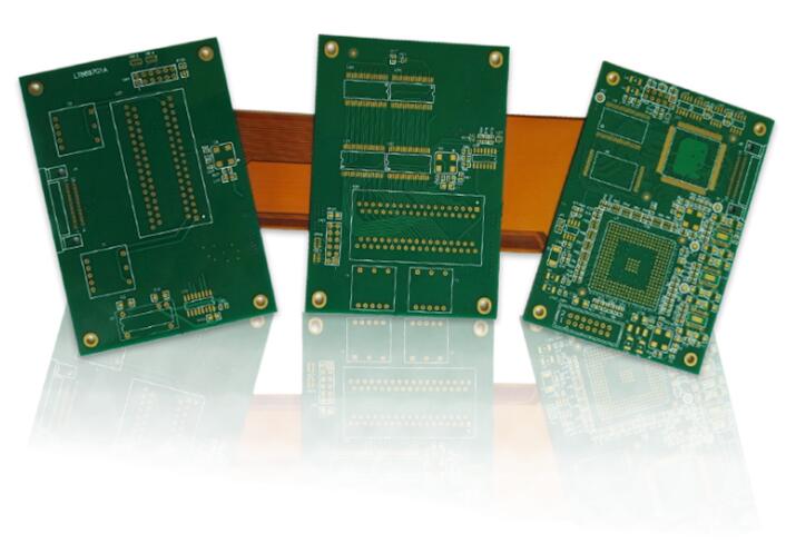
Printed circuit boards (PCBs) are an essential part of modern electronic devices, providing reliable electrical interconnections between components, sub-boards, and mainboards. Depending on their construction and application requirements, PCBs can generally be categorized into rigid PCB, rigid-flex PCB, and flexible PCB. Among these technologies, flexible PCB solutions have become increasingly…
Printed circuit boards can generally be divided into two major categories: rigid PCB and flexible PCB. As their names suggest, rigid PCBs maintain a fixed shape, while flexible PCBs can bend, fold, or conform to three-dimensional structures according to the requirements of the end product. Both technologies remain widely used…