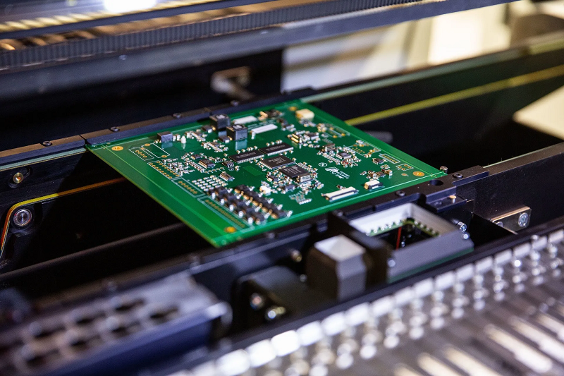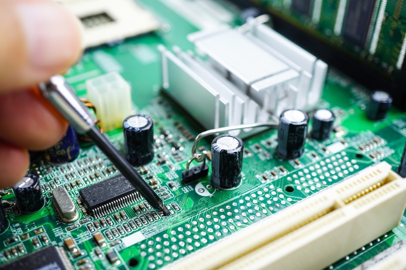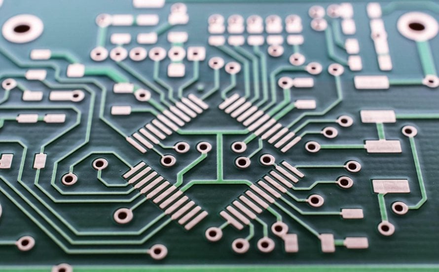
PCB Design and Component Layout for High Performance High performance on a circuit board is rarely an accident. It starts with a placement decision, a return path, and a stackup that someone planned before routing began. When a design fails in the lab, the cause is often visible in the…
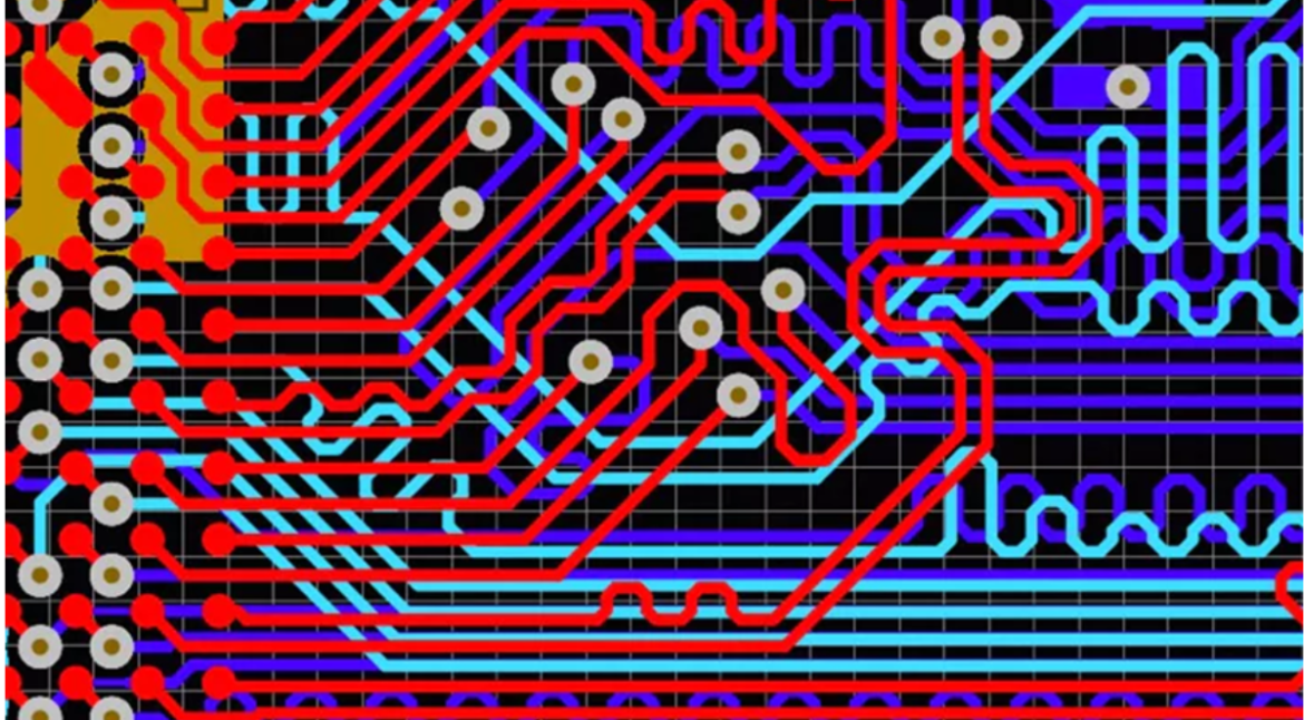
PCB Impedance Control for High-Speed Performance A high-speed board rarely fails on the schematic. It fails where a trace width drifts, a dielectric thickness shifts, or a reference plane is cut by a routing decision. Impedance control turns those physical details into a specified target and a measured result. The…
PCB Thermal Design Guide for Small Batch Builds Heat is the quiet limit on most boards. A design that runs cool in the lab can drift once it sits in an enclosure with poor airflow and a warm ambient. Thermal choices are made early, in copper, stackup, vias and placement,…
HDI PCB Browning and Copper Peeling Causes Copper peeling on an HDI board rarely starts at the moment the trace lifts. The separation usually begins earlier, at the interface between copper and resin, where a browning line set slightly wrong left a weak bond. Builders who understand the browning process…
COB Packaging on HDI PCB: Features and Proofing Checks Bare dies bonded straight onto a dense board change what a prototype must prove. Chip on board removes the plastic package, so the PCB surface becomes the package. On an HDI stackup, that shift touches pad finish, wire bond placement, encapsulation…
Multilayer PCB and High TG PCB Materials Guide Multilayer boards and high TG laminates solve two different problems, yet buyers often treat them as one line item. The layer count sets routing density and impedance control needs. The resin system sets how much heat the board survives during assembly and…
In modern electronics, Control PCBs have become an essential part of systems that require intelligent signal processing, monitoring, automation, and decision-making. Unlike conventional PCBs that primarily provide electrical connections between components, a control PCB integrates processing devices, communication interfaces, power management circuits, sensors, and input/output interfaces to control the operation…
OSP Surface Finish for PCB Manufacturing OSP is a thin organic film that protects exposed copper before assembly. It keeps the pad surface solderable and flat until the board reaches the reflow oven. Engineers choose it when fine-pitch parts and dense routing leave little room for a thick coating. Buyers…
Blind and Buried Vias in PCB: Design, Manufacturing, Applications, and Key Differences Blind and buried vias are essential technologies in advanced multilayer PCB and HDI PCB design. As electronic devices become smaller, more powerful, and more densely integrated, conventional through-hole vias can consume valuable routing space and limit component placement.…
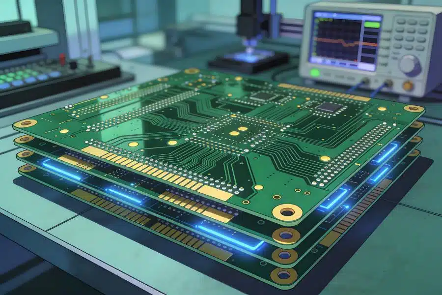
4-Layer PCB: Stackup, Design, Manufacturing Process, Applications, and Cost As modern electronic products become increasingly compact and functionally complex, PCB design must accommodate higher component density, faster signal transmission, improved power distribution, and better electromagnetic compatibility. For many applications, a 4-layer PCB provides an effective balance between electrical performance, design…