HDI PCB Browning Process and Causes of PCB Copper Peeling
With the continuous development of electronic products toward miniaturization, higher performance, and greater reliability, HDI PCB technology has become an essential solution for advanced electronic applications. High-density interconnect boards require precise manufacturing processes to ensure strong layer bonding, stable electrical performance, and long-term reliability.
During PCB Manufacturing, surface treatment processes such as browning and blackening play an important role in improving the bonding strength between copper layers and resin materials. However, improper processing or unsuitable materials may cause defects such as PCB Copper Peeling, which can seriously affect product performance.
Understanding the causes and prevention methods of copper peeling helps engineers optimize PCB Design and improve manufacturing quality.
For professional circuit board production solutions, explore our PCB Manufacturing Service.
What Is the Browning Process in HDI PCB Manufacturing?
The browning process is a surface treatment technology used during HDI PCB production to enhance the bonding strength between the copper surface and prepreg materials.
Before multilayer lamination, the copper surface needs to be treated to improve adhesion. The browning process creates a uniform micro-rough structure on the copper surface, increasing the contact area between copper foil and resin.
The main purposes of the browning process include:
1. Removing Surface Contaminants
During production, copper surfaces may contain oil, dust, oxidation residues, or other contaminants. The browning process cleans the copper surface to ensure better bonding performance.
2. Increasing Copper and Resin Adhesion
After browning treatment, a microscopic rough layer forms on the copper surface. This structure allows resin materials to penetrate into the surface during lamination, improving the mechanical bonding force.
3. Improving Multilayer PCB Reliability
A properly treated copper surface reduces the risk of delamination, layer separation, and board explosion during high-temperature processing.
This process is especially important for high-layer-count boards and complex HDI PCB structures.
Difference Between Browning and Blackening Treatment
Both browning and blackening processes are designed to improve copper-resin adhesion, but there are several differences between them.
Similarities Between Browning and Blackening
Both treatments provide the following benefits:
- Increase the contact area between copper foil and resin
- Improve surface wettability
- Enhance bonding strength after lamination
- Reduce the possibility of PCB layer separation
Differences Between Browning and Blackening
Surface Structure
The thickness and structure of the treated copper surface are different. Blackening usually creates a thicker oxide layer compared with browning treatment.
Process Control
The chemical solution used for blackening requires stricter control compared with browning because variations can have a greater impact on surface quality.
Cost Considerations
Blackening treatment generally has higher processing costs, while browning provides a more economical solution for many PCB Manufacturing applications.
Surface Roughness
Blackened surfaces usually have higher roughness, which may provide stronger adhesion. However, excessive roughness may affect fine circuit structures in advanced PCB applications.
Common Causes of PCB Copper Peeling Problems
PCB Copper Peeling refers to the separation of copper traces from the substrate material. This defect can cause open circuits, reduced reliability, and product failure.
Several factors may contribute to copper peeling.
Manufacturing Process Factors
Excessive Copper Etching
During PCB fabrication, excessive etching can reduce the thickness of copper traces and weaken their connection with the substrate.
Improper etching control may result in:
- Narrower circuit lines
- Reduced copper strength
- Higher risk of trace separation
Precise process management is required during PCB Manufacturing to avoid these issues.
Mechanical Damage During Production
During handling, transportation, or processing, mechanical impact may damage the copper layer.
Common signs include:
- Copper trace deformation
- Scratches on the circuit surface
- Local copper separation
Strict production control and automated inspection help reduce these risks.
PCB Design Related Causes
Improper PCB Design can also increase the possibility of copper peeling.
For example:
- Extremely thin traces combined with thick copper layers
- Poor copper distribution
- Incorrect thermal design
- Excessive current loading on narrow traces
Engineers should optimize circuit layout based on electrical requirements and manufacturing capabilities.
For professional design support, visit our PCB Design Service.
PCB Laminate Manufacturing Factors
The quality of laminate materials directly affects copper adhesion.
During multilayer pressing, copper foil and prepreg materials must form a strong bond. Problems may occur when:
- Prepreg materials are contaminated
- Copper surfaces are damaged before lamination
- Pressing temperature or pressure is insufficient
These issues can weaken the connection between copper foil and substrate.
Using reliable PCB Substrate materials and controlled lamination processes helps improve board reliability.
Raw Material Factors Affecting Copper Adhesion
Copper Foil Quality

Copper foil is a critical material in PCB production. Poor-quality copper foil may have insufficient peel strength due to:
- Improper surface treatment
- Abnormal roughness
- Poor electroplating quality
When defective copper foil is used, copper traces may separate during assembly or operation.
Compatibility Between Copper Foil and Resin
The copper foil and resin system must have good chemical compatibility.
If the materials do not match properly, the bonding strength may decrease, resulting in:
- Copper peeling
- Layer separation
- Reduced PCB reliability
Material selection is especially important for high-performance applications.
Learn more about advanced board materials through our PCB Material Solutions.
How to Prevent PCB Copper Peeling
To improve PCB reliability, manufacturers should focus on several key areas.
Optimize Surface Treatment Processes
Proper control of browning or blackening parameters ensures strong copper-resin bonding.
Important factors include:
- Chemical concentration
- Processing time
- Surface cleanliness
- Storage conditions after treatment
Improve PCB Design Quality
Engineers should consider manufacturing requirements during the design stage.
Recommended practices include:
- Maintaining suitable trace width
- Avoiding excessive copper density differences
- Following manufacturer design guidelines
- Performing design rule checks
Select High-Quality Materials
Using reliable copper foil, prepreg, and laminate materials improves long-term performance.
High-quality PCB Substrate materials provide:
- Better thermal stability
- Stronger copper adhesion
- Improved mechanical reliability
The Importance of Quality Control in PCB Manufacturing
Modern electronics require highly reliable circuit boards. A professional supplier should implement strict quality control throughout the entire production process.
Key inspection steps include:
- Incoming material inspection
- Copper thickness measurement
- Surface treatment inspection
- Lamination testing
- Electrical testing
- Final quality verification
Advanced manufacturing management ensures stable performance for applications such as automotive electronics, medical devices, industrial equipment, and communication systems.
Explore our complete PCB Assembly Service for reliable production support.
Conclusion
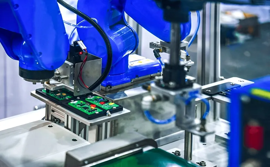
The browning process is a critical step in HDI PCB manufacturing because it improves copper and resin bonding strength, helping prevent delamination and reliability issues.
At the same time, PCB Copper Peeling can result from multiple factors, including manufacturing processes, material selection, and improper PCB Design.
By using high-quality PCB Substrate materials, optimizing manufacturing processes, and applying strict quality control, manufacturers can significantly improve PCB performance and durability.
Reliable PCB Manufacturing requires advanced technology, experienced engineering teams, and effective process management to deliver high-quality circuit board solutions for modern electronics.