KingdaKingdaKingda

Call Us 24/7

+86-181-2376-9076

Send Us Mail

sales@gopcba.com

Our Location

Baoan District, Shenzhen, China

Language

  • enEnglish
    • fr France
    • itItalian
Kingda
  • Home
  • PCB Assembly
    • Prototype PCB Assembly
    • Turnkey PCB Assembly
    • Low Volume PCB Assembly
    • High Volume PCB Assembly
    • SMT PCB Assembly
    • Through Hole PCB Assembly
    • Mixed Technology PCB Assembly
    • Flex PCB Assembly
  • Services
    • PCB Design/Layout
    • PCB Manufacturing
    • Rapid PCBA Prototyping
    • Components Procurement
    • Conformal Coating
    • PCBA Testing
    • Box Build Assembly
    • Wire & Cable Harness Assembly
  • Industry Solutions
    • Medical PCBA
    • Telecommunications PCBA
    • Energy PCBA
    • Industrial PCBA
    • Artificial Intelligence PCBA
    • IOT PCBA
  • Resources
    • PCB Capabilities
    • PCBA Capabilities
    • FAQ
    • Blog
  • About Us
    • About Us
    • Why Us
    • Quality Management
    • Our PCB Assembly Process
  • Contact Us
Get A Quote
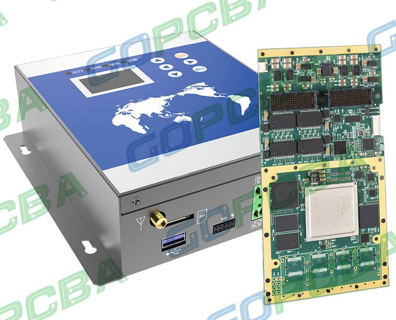
无线遥测终端PCBA

Solder Mask Spray Coating: 6 Rules for Even Films

  • By Frank guo
  • 2026年 9月 13日
  • PCB Assembly
  • No Comments
Solder Mask Spray Coating: 6 Rules for Even Films Solder mask spray coating builds the protective film by atomizing liquid ink and depositing it on the panel surface, layer by layer, instead of pushing it through a screen. It is chosen where the copper is tall, the features are dense…
Continue Reading
High-Speed PCB Design, Manufacturing, and Assembly

PCB Statement of Work Specification: Writing It Down Precisely

  • By 杰夫
  • 2026年 9月 13日
  • PCB Assembly
  • No Comments
PCB Statement of Work Specification: Practical Process Controls Modern electronics depend on boards that are assembled correctly the first time. Every product – a phone, a charger, a medical instrument or an industrial controller – relies on thousands of solder joints that must conduct current for years. This article explains…
Continue Reading
ptt_history

Solder Mask Jetting: Inkjet Printing for Fine Features

  • By Frank guo
  • 2026年 9月 13日
  • PCB Assembly
  • No Comments
Solder Mask Jetting: Inkjet Printing for Fine Features Solder mask jetting is the deposition of solder mask ink directly onto the board through an inkjet print head, with no screen, no film and no development step. The head writes the pattern from the CAD data, so a change to a…
Continue Reading
PCB conformal coating

PCB Statement of Work Sample: Checking a Small Piece

  • By 杰夫
  • 2026年 9月 13日
  • PCB Assembly
  • No Comments
PCB Statement of Work Sample: From Design to Repeatable Production Electronics manufacturing has become a discipline of small details. Solder paste volumes, placement accuracy, temperature profiles and inspection limits all add up to the final result. This guide looks at PCB statement of work sample from the perspective of a…
Continue Reading
wave-overlay

Etchant Analysis: Keeping Copper Etch Chemistry in Balance

  • By Frank guo
  • 2026年 9月 13日
  • PCB Assembly
  • No Comments
Etchant Analysis: Keeping Copper Etch Chemistry in Balance Etchant analysis is the routine measurement of the chemistry that dissolves copper, and it exists because the etch rate drifts as copper accumulates and the oxidising power of the bath falls. A bath that is not analysed etches slowly at the start…
Continue Reading
PCB Assembly

Steam Aging for Solderability Testing: 7 Process Rules

  • By Frank guo
  • 2026年 9月 13日
  • PCB Assembly
  • No Comments
Steam Aging for Solderability Testing: 7 Process Rules Steam aging is a preconditioning step rather than a test in itself. It exposes a test coupon to hot, condensing moisture for a defined period so that the surface oxide grows in hours to something like the condition a board would reach…
Continue Reading
219

Lead Tinning: 6 Rules for Component Solderability

  • By Frank guo
  • 2026年 9月 13日
  • PCB Assembly
  • No Comments
Lead Tinning: 6 Rules for Component Solderability Lead tinning is the operation that replaces a component lead finish with fresh solder so that the part can be soldered reliably in a later assembly step. It is common on parts with aged, oxidised or incompatible finishes, and on hardware and connectors…
Continue Reading
section-3

Laminography: 3D X-Ray Imaging for Solder Joints

  • By Frank guo
  • 2026年 9月 13日
  • PCB Assembly
  • No Comments
Laminography: 3D X-Ray Imaging for Solder Joints Laminography, also called computed laminography or tomosynthesis, produces an X-ray image of one plane inside an assembly while the material above and below that plane is blurred out. The result is a view of a single solder joint layer without the superposition that…
Continue Reading
PCB Assembly

Tin Pest in PCB Finishes: 6 Rules for Cold Storage and Alloys

  • By Frank guo
  • 2026年 9月 13日
  • PCB Assembly
  • No Comments
Tin Pest in PCB Finishes: 6 Rules for Cold Storage and Alloys Tin pest is the transformation of white tin, the familiar ductile metal, into grey tin, a brittle phase that crumbles to powder. The change becomes possible below about thirteen degrees Celsius, it is slow at first and then…
Continue Reading
PCB Pad Design

Trace Repair and Jumper Wires on PCB Assemblies: 7 Rules

  • By Frank guo
  • 2026年 9月 13日
  • PCB Assembly
  • No Comments
Trace Repair and Jumper Wires on PCB Assemblies: 7 Rules A trace repair is the last resort before a board is scrapped. A conductor that has been cut by a probe, torn during rework or cracked by repeated flexing can often be restored, but the repair has to carry the…
Continue Reading
1 … 429 430 431 … 1,621

Search Posts

Categories

  • Electronic Materials
  • Electronical Engineering
  • Industrial Control
  • PCB Assembly
  • PCB Design
  • PCB Manufacturing

Recent Posts

Low-Temperature Solder for LED Modules: Thermal Budget and Joint Reliability

Frank guo - 2026年 11月 6日
Surface Mount Technology (SMT): Process, Components, Design Guidelines & PCB Assembly

Surface Mount Technology (SMT): Process, Components, Design Guidelines & PCB Assembly

Zane Zhang - 2026年 10月 2日
Cheap PCB Costs: PCB Design, PCB Manufacturing & SMT vs TH Guide

Cheap PCB Costs: PCB Design, PCB Manufacturing & SMT vs TH Guide

Jelly - 2026年 9月 30日

Tags

AOI inspection automotive electronics automotive PCBA quality automotive standards box build assembly component procurement component supplier conformal coating defect prevention DFM checks DFM review e-bom management electronic component shortage electronic manufacturing services electronic manufacturing standards Electronic Materials electronics design best practice electronics manufacturing capacity electronics sourcing high volume production industrial electronics manufacturability review mass production quality mixed technology PCB PCBA inspection PCBA prototype PCBA turnkey PCBA volume pricing PCB Design PCB layout rules PCB Manufacturing PCB sourcing power electronics PCB printed circuit board prototype quick turn PCB reflow soldering reflow soldering profile SMT assembly quality SMT production soldering defect analysis solder joint quality solder paste inspection solder paste printing surface mount technology vehicle electronics
GOPCBA-logo

As a professional China PCB assembly manufacturer, we provide a full range of electronic manufacturing services from PCB fabrication, PCBA to OEM/ODM, including PCB design, PCB layout, rapid PCBA prototyping, components procurement, SMT/ THT assembly, china pcb assembly, china pcb prototype, PCBA testing and box build assembly.

Linkedin Facebook-f X-twitter Youtube Instagram

PCB ASSEMBLY

  • Prototype PCB Assembly
  • Low Volume PCB Assembly
  • High Volume PCB Assembly
  • Turnkey PCB Assembly
  • SMT PCB Assembly
  • Through Hole PCB Assembly
  • Mixed Technology PCB Assembly
  • Flex PCB Assembly

OUR SERVICES

  • PCB Design/Layout
  • PCB Manufacturing
  • Rapid PCBA Prototyping
  • Components Procurement
  • Conformal Coating
  • PCBA Testing
  • Box Build Assembly
  • Wire & Cable Harness Assembly

TECHNICAL SUPPORT

  • About Us
  • Quality Management
  • Artificial Intelligence PCBA
  • Industrial PCBA
  • IOT PCBA
  • Medical PCBA
  • Energy PCBA
  • Telecommunications PCBA

Copyright © 2026. Shenzhen Kingda Electronics Co., LTD  All rights reserved. 

  • Sitemap
  • Terms of Service
  • Privacy Policy
Zmdi Zmdi-email Phone-square Whatsapp Weixin
x

ABOUT US

Progressively maintain extensive infomediaries via extensible nich. Capitalize on low hanging fruit. a ballpark value added is activity to beta test. Override the digital divide with additional click throughs from fruit.

LOCATIONS

map

Shenzhen Office

+86-181-2376-9076
sales@gopcba.com
3rd Floor, Building 11, Houting Third Industrial Zone, Shajing Avenue, Baoan District, Shenzhen, China.
Contact Us

FOLLOW US