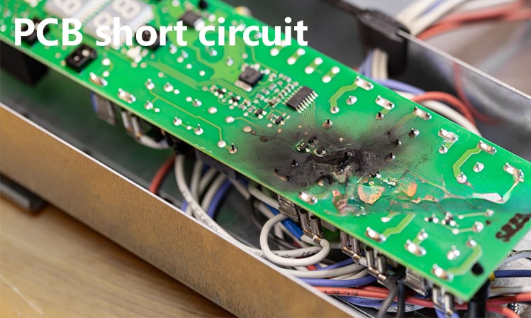
When Layout Decisions Become Signal Integrity Problems A schematic can be complete, correct and fully verified, and the board built from it can still fail at the first eye measurement. The reason is that a schematic describes connectivity, not geometry. It does not say which layer a net travels on,…
100 MHz vs 1 GHz: High Speed Interfaces on the PCB An interface running at a hundred megahertz and one running at a gigahertz are separated by a factor of ten in clock rate, and by much more than that in layout difficulty. The difference is not simply that high…
Unified EDA Data Model Versus a Distributed Toolchain Hardware design has traditionally been a chain of specialised tools. Schematic capture, PCB layout, power and signal integrity simulation, and manufacturability checking each live in their own environment, connected by exported files. The workflow is familiar, but it carries a structural cost:…
PCB Panelization: Size, Spacing and Material Utilization The panel a board is built on is a shared resource, and the way a design is arranged on it decides how much of the raw material is converted into product and how much is thrown away. That arrangement is usually the shop’s…
4-Layer RF PCB Cost: Materials, Stackup and Volume Four layers is the most common stackup for RF work in the low gigahertz range, because it is the smallest construction that gives a microstrip line on the top layer, a solid reference immediately below it, and two more layers for power…
Bare Pcb Manufacturing Cost: Preparation, Placement and Process Control A bare board is a PCB with no components on it, and its price is the clearest view of what fabrication actually costs. Stripping the assembly out of the quotation removes the component and labour noise, leaving laminate, copper, chemistry, drilling,…
PCB Layout Order: Four Position Classes to Fix Before Routing Most first-pass layout sessions stall for the same reason: the schematic is finished, the netlist is imported, and a screen full of rat’s nest lines gives no hint about which part should move first. Some engineers drop the largest chip…
Why Adding Copper Pour Changes Trace Impedance Adding copper beside a trace seems like a harmless improvement. It lowers resistance, spreads heat, gives the etchant something to work against and makes the board look finished. Then the impedance measurement comes back below target, and the reason is that the new…
Conformal Coating vs Potting: Choosing PCB Protection Protecting a finished assembly from moisture, contamination and mechanical damage is a design decision with a cost consequence, and the two common answers behave very differently. A thin coating follows the board, while potting surrounds it. This guide explains when each is appropriate,…
Bare PCB Manufacturing Cost: What a Blank Board Costs A bare board is a PCB with no components on it, and its price is the clearest view of what fabrication actually costs. Stripping the assembly out of the quotation removes the component and labour noise, leaving laminate, copper, chemistry, drilling,…