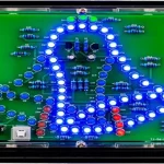
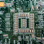
Electronics have become an essential part of modern life. From smartphones and computers to automobiles, industrial equipment, medical devices, and communication systems, almost every electronic product relies on a printed circuit board (PCB) to connect and control its electronic components.
A PCB is the foundation of an electronic product. It provides mechanical support for components while creating electrical connections between them through conductive copper traces. However, a bare PCB alone cannot perform its intended electronic functions. Components must be accurately mounted and soldered onto the board before it becomes a functional electronic assembly.
A PCB populated with electronic components is called a printed circuit board assembly (PCBA), and the manufacturing process is known as PCB assembly or PCBA manufacturing.
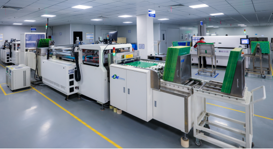
During PCB assembly, components such as resistors, capacitors, diodes, integrated circuits (ICs), connectors, sensors, and other electronic devices are mounted onto a PCB. Depending on the product design, manufacturers may use surface mount technology (SMT), through-hole technology (THT), or a combination of both.
Modern PCB assembly services involve much more than simply placing components on a circuit board. The complete process can include DFM review, solder paste printing, component placement, reflow soldering, through-hole insertion, wave soldering, AOI, X-ray inspection, functional testing, cleaning, programming, and final quality control.
As an experienced PCB manufacturer and PCB assembly service provider, Kingda provides PCB prototyping, quick-turn PCB manufacturing, component sourcing, and PCB assembly solutions, supporting customers from initial design verification through full-scale production.
The following guide explains the PCB assembly process step by step.
PCB Design Basics
The PCBA process begins with the PCB itself. A PCB typically consists of several functional layers, and each layer contributes to the electrical, mechanical, and manufacturing performance of the finished board.
The primary PCB layers include:
Substrate
The substrate is the structural foundation of the PCB. It provides mechanical strength and determines many of the board’s thermal and electrical characteristics.
FR-4 fiberglass-reinforced epoxy laminate is one of the most widely used PCB substrate materials. Depending on the application, manufacturers may also use high-Tg materials, polyimide, Rogers materials, aluminum substrates, and other specialized materials.
Copper Layer
A thin layer of conductive copper foil is laminated onto the PCB substrate. Copper is patterned to form PCB traces, pads, planes, and other conductive structures.
Single-sided PCBs have conductive copper on one side, while double-sided and multilayer PCBs contain copper layers on multiple levels.
Solder Mask
The solder mask is an insulating protective layer applied over the copper traces. It helps prevent accidental electrical contact, protects copper from oxidation, and reduces the possibility of solder bridges during PCB assembly.
Although green is the most common solder mask color, other colors are also available depending on design and application requirements.
Silkscreen
The silkscreen is the printed identification layer on the PCB. It commonly contains component reference designators, polarity markings, logos, labels, and other information that helps operators and engineers identify components during assembly, inspection, testing, and maintenance.
These PCB layers work together to provide the electrical connectivity, mechanical support, and protection required for reliable electronic products.
Major Types of PCBs
Different electronic applications require different PCB structures and materials. The three common PCB categories include rigid PCBs, flexible PCBs, and metal core PCBs.
Rigid PCB
A rigid PCB is the most widely used PCB type. Its solid structure provides mechanical stability and dimensional consistency.
FR-4 is the most common rigid PCB material and is widely used in consumer electronics, industrial equipment, telecommunications, automotive electronics, and many other applications.
Depending on the design, rigid PCBs can be manufactured as single-sided, double-sided, or multilayer boards.
Flexible PCB
A flexible PCB, or FPC, uses a flexible substrate that allows the circuit to bend, fold, or conform to a specific product shape.
Polyimide is commonly used as the base material for flexible circuits. Flexible PCBs are particularly useful in compact electronic products, wearable devices, displays, cameras, automotive electronics, and applications where space and mechanical movement are important.
Metal Core PCB
A metal core PCB incorporates a metal base, commonly aluminum, to improve thermal dissipation.
Metal core PCBs are frequently used in high-power applications such as LED lighting, power electronics, automotive systems, and other products where efficient heat management is essential.
SMT and THT Assembly Technologies
Modern PCB assembly manufacturing mainly uses two component mounting technologies: surface mount technology (SMT) and through-hole technology (THT).
Surface Mount Technology (SMT)
SMT assembly mounts electronic components directly onto the surface of the PCB.
Surface-mount devices (SMDs) are available in extremely compact packages, making SMT ideal for high-density electronic designs.
Common SMT components include:
- Resistors
- Capacitors
- Diodes
- Transistors
- ICs
- Microcontrollers
- Sensors
- RF components
- Power management devices
Because SMT assembly can be highly automated, it provides excellent manufacturing efficiency, repeatability, and component placement accuracy.
Modern SMT equipment can handle extremely small packages, including 0201 and, for suitable applications, 01005 components.
Through-Hole Technology (THT)
Through-hole technology (THT) installs components by inserting their leads through holes drilled into the PCB.
THT components are often selected when mechanical strength, high-current capability, or specific component package requirements are important.
Common THT components include:
- Large capacitors
- Transformers
- Connectors
- Relays
- Switches
- Power components
- Mechanical components
After insertion, the component leads are soldered to the PCB, commonly using wave soldering or selective soldering.
Mixed Technology Assembly
Many modern electronic products require both SMT and THT components. In these cases, manufacturers use mixed technology PCB assembly.
Mixed assembly allows designers to combine the high-density advantages of SMT with the mechanical and electrical advantages of THT.
The appropriate assembly sequence depends on component placement, PCB design, thermal requirements, soldering constraints, and production volume.
Before the PCB Assembly Process
Before physical assembly begins, several engineering and preparation activities must be completed.
A professional PCB assembly manufacturer normally requires the PCB design files, bill of materials (BOM), component specifications, assembly drawings, Gerber files, pick-and-place files, and other manufacturing instructions.
DFM and DFA Review
A Design for Manufacturability (DFM) review identifies potential PCB fabrication and assembly problems before production begins.
A Design for Assembly (DFA) review focuses on whether components can be efficiently and reliably assembled.
Typical checks include:
- Component spacing
- Pad dimensions
- Solder mask clearance
- Via placement
- PCB edge clearance
- Component orientation
- Fiducial placement
- Soldering accessibility
- Thermal considerations
- Component availability
- Manufacturing tolerances
Identifying problems during the engineering stage can reduce PCB assembly costs, minimize rework, shorten production lead times, and improve first-pass yield.
Kingda can provide engineering review and manufacturing feedback before production, helping customers identify potential design and assembly issues at an early stage.
PCB Assembly Process Steps
The exact PCBA manufacturing process varies according to PCB structure, component type, product requirements, and production volume. However, a typical SMT/THT assembly process includes the following steps.
Step 1: Solder Paste Printing
The first major step in the SMT PCB assembly process is solder paste printing.
A stainless-steel stencil is positioned over the PCB. Solder paste is then applied across the stencil using a controlled printing process.
The stencil contains precisely defined openings corresponding to the PCB’s solder pads. When the stencil is lifted, solder paste remains only on the designated pads.
The quality of solder paste printing directly affects subsequent soldering quality.
Key factors include:
- Stencil thickness
- Aperture design
- Squeegee pressure
- Printing speed
- Paste viscosity
- PCB alignment
- Environmental conditions
For advanced PCB assembly, Solder Paste Inspection (SPI) can be used to verify solder paste volume, height, alignment, and coverage before components are placed.
Step 2: Pick-and-Place Component Mounting
After solder paste printing, the PCB moves to the pick-and-place machine.
The automated placement machine retrieves components from reels, trays, or other feeders and places them onto the corresponding PCB pads.
Modern pick-and-place equipment uses high-speed vision systems to identify component position, orientation, and package characteristics.
Automated placement provides several important advantages:
- High placement accuracy
- Consistent production quality
- High throughput
- Reduced manual handling
- Improved repeatability
- Support for miniature components
The component placement program is generated from the PCB design and pick-and-place data, ensuring that each component is installed at its designated location.
Step 3: Reflow Soldering
After component placement, the PCB passes through a reflow soldering oven.
The board moves through multiple controlled temperature zones. The solder paste first undergoes preheating and thermal soaking before reaching a temperature high enough to melt the solder alloy.
Once the solder melts, it forms reliable solder joints between the component terminals and PCB pads. The board is then cooled under controlled conditions.
A properly developed reflow profile is essential for achieving reliable solder joints while preventing thermal damage to components and the PCB.
For complex boards, the reflow profile may be optimized according to:
- PCB thickness
- Component package types
- PCB material
- Solder paste specifications
- Thermal mass
- Component temperature limitations
For double-sided SMT assembly, each side is processed according to the specific component arrangement and thermal requirements.
Step 4: Inspection and Quality Control
Reflow soldering does not mean that the PCB assembly process is complete. The assembled board must be inspected to identify soldering defects, component misalignment, missing components, polarity errors, and other potential problems.
Professional PCB assembly manufacturers commonly combine several inspection technologies.
Manual Visual Inspection
Manual inspection can be useful for prototypes, engineering samples, and low-volume PCB assembly.
Experienced operators can identify visible problems such as:
- Incorrect component orientation
- Missing components
- Damaged components
- Obvious solder bridges
- Incorrect assembly
- Mechanical damage
However, manual inspection alone becomes less practical as component density and production volume increase.
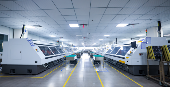
Automated Optical Inspection (AOI)
Automated Optical Inspection (AOI) uses cameras and image-processing technology to inspect PCB assemblies automatically.
AOI can identify defects such as:
- Missing components
- Incorrect components
- Component displacement
- Polarity errors
- Solder bridges
- Insufficient solder
- Excessive solder
- Incorrect solder joints
AOI is especially valuable for medium- and high-volume PCB assembly production, where consistent inspection speed and repeatability are important.
X-Ray Inspection
X-ray inspection is particularly useful for components and solder joints that cannot be fully inspected from the PCB surface.
Typical applications include:
- BGA packages
- QFN packages
- Hidden solder joints
- Bottom-terminated components
- Complex multilayer assemblies
X-ray inspection provides visibility into internal solder connections and can help identify voids, bridging, insufficient solder, and other hidden defects.
Step 5: Through-Hole Component Insertion
If the PCB design includes THT components, they are installed after or alongside the SMT process according to the required assembly sequence.
Through-hole components are inserted into the designated plated through-holes on the PCB.
Depending on production requirements, insertion may be performed manually or using automated equipment.
THT components are often selected for applications requiring:
- High mechanical strength
- High current carrying capability
- Large component packages
- Robust connectors
- Power components
After insertion, the component leads are soldered to the PCB.
Wave Soldering
Wave soldering is a widely used automated process for soldering through-hole components.
The PCB passes over a controlled wave of molten solder, allowing solder to contact exposed component leads on the underside of the board.
Wave soldering is highly efficient for suitable THT assemblies, particularly in higher-volume production.
Selective Soldering
For mixed-technology PCB assemblies, selective soldering can be used when only specific through-hole components need to be soldered.
Unlike wave soldering, selective soldering applies molten solder only to designated locations. This helps protect nearby SMT components and makes the process suitable for complex mixed-technology boards.
Step 6: Final Inspection and Functional Testing
After all components have been assembled and soldered, the finished PCBA undergoes final inspection and testing.
Depending on the product requirements, testing can include:
In-Circuit Test (ICT)
ICT checks electrical characteristics and specific circuit nodes to identify manufacturing defects such as open circuits, short circuits, incorrect component values, and certain component placement problems.
Flying Probe Test
Flying probe testing uses movable probes to test electrical connections without requiring a dedicated fixture.
It is particularly suitable for prototypes, new product introduction (NPI), and low-volume PCB assembly.
Functional Test (FCT)
A functional test evaluates whether the assembled PCB performs according to its intended operating specifications.
The PCBA may be powered and connected to simulated input and output signals while key electrical parameters are monitored.
Depending on the product, functional testing can evaluate:
- Voltage
- Current
- Signal output
- Communication interfaces
- Sensor operation
- Power management
- System functions
Programming and Calibration
Many modern PCB assemblies require firmware programming or calibration before shipment.
Kingda can support appropriate PCB assembly and testing requirements, including production programming and product-specific inspection processes where required.
Step 7: PCB Cleaning
After soldering, flux residues and other contaminants may remain on the PCB surface.
Depending on the solder paste, flux type, application, and customer requirements, PCB cleaning may be required.
Professional PCB cleaning processes can use specialized cleaning equipment and suitable cleaning agents to remove:
- Flux residues
- Ionic contaminants
- Solder particles
- Dust
- Handling contaminants
The cleaning method must be selected according to PCB materials, components, coatings, and end-product requirements.
After cleaning, the PCB assembly is thoroughly dried before final inspection and packaging.
Step 8: Final Quality Control, Packaging, and Shipment
Before shipment, the completed PCB assemblies undergo final quality verification.
The final inspection may include:
- Visual inspection
- Dimensional verification
- Component verification
- Solder joint inspection
- Electrical testing
- Functional testing
- Label verification
- Packaging inspection
Proper packaging is particularly important for sensitive electronic assemblies.
Depending on the product, manufacturers may use ESD-safe packaging, moisture protection, protective trays, vacuum packaging, or customized packaging solutions.
Differences Between SMT, THT, and Mixed PCB Assembly
The three primary PCB assembly approaches can be summarized as follows:
| Assembly Technology | Main Process | Typical Components | Key Advantages |
|---|---|---|---|
| SMT Assembly | Solder paste printing → Pick and place → Reflow soldering | Resistors, capacitors, ICs, sensors | High density, automation, high efficiency |
| THT Assembly | Component insertion → Wave/selective/manual soldering | Connectors, relays, transformers, power components | Strong mechanical connection |
| Mixed Technology | SMT + THT processes | Complex electronic assemblies | Combines SMT density with THT strength |
SMT Assembly
The typical SMT assembly process is:
Solder Paste Printing → SPI → Pick and Place → Reflow Soldering → AOI → X-Ray/Testing
SMT is widely used in compact and high-density electronic products.
THT Assembly
The typical THT assembly process is:
Component Insertion → Inspection → Wave/Selective Soldering → Inspection → Testing
THT is often used for components requiring strong mechanical connections or higher power handling.
Mixed Technology Assembly
Mixed technology assembly combines SMT and THT components on the same PCB.
A typical workflow may include:
SMT Printing → SMT Placement → Reflow → THT Insertion → Selective/Wave Soldering → Inspection → Testing
The actual sequence depends on component locations, PCB structure, soldering requirements, and product specifications.
How to Choose a Reliable PCB Assembly Manufacturer
Choosing a suitable PCB assembly manufacturer is critical because manufacturing capability directly affects product quality, cost, lead time, and long-term reliability.
When evaluating a PCB assembly supplier, consider the following factors:
Manufacturing Capability
Check whether the supplier can support the PCB technologies required by your project, including:
- Single-sided PCB
- Double-sided PCB
- Multilayer PCB
- HDI PCB
- Rigid-flex PCB
- Flexible PCB
- SMT assembly
- THT assembly
- Mixed technology assembly
Component Sourcing Capability
A reliable PCB assembly service provider should have the capability to source components according to the approved BOM.
Professional component procurement helps reduce risks related to:
- Counterfeit components
- Obsolete components
- Component shortages
- Long lead times
- Unauthorized substitutions
Quality Control
A strong quality management system should cover the entire manufacturing process, from PCB fabrication and component sourcing to assembly, inspection, testing, and shipment.
Important quality tools may include:
SPI → AOI → X-Ray → ICT/Flying Probe → Functional Testing → Final Inspection
Engineering Support
A capable PCB assembly partner should provide engineering support rather than simply manufacturing files without review.
DFM/DFA analysis, BOM review, component availability checks, and assembly optimization can help identify potential problems before production.
Scalability
The supplier should be capable of supporting the product through different development stages:
PCB Prototype → NPI → Small-Batch Production → Volume Manufacturing
This allows customers to maintain a stable manufacturing relationship as their product moves from development into commercial production.
Kingda PCB Assembly Services
As an experienced PCB manufacturer and PCB assembly service provider, Kingda provides integrated solutions designed to support customers throughout the electronics manufacturing lifecycle.
Our capabilities can cover the process from initial design verification and PCB prototyping to component sourcing, PCB assembly, inspection, testing, and production.
Kingda’s PCB Assembly Advantages
1. One-Stop PCB and PCBA Solutions
Kingda can integrate PCB fabrication and PCB assembly, helping simplify supplier management and coordinate manufacturing processes.
2. PCB Prototype and Quick-Turn Manufacturing
For new electronic products, fast prototype manufacturing can help engineers verify circuit designs, identify potential issues, and accelerate product development.
3. SMT, THT, and Mixed Technology Assembly
Kingda supports different assembly requirements, including SMT assembly, through-hole assembly, and mixed-technology PCB assembly, according to individual product specifications.
4. Engineering and DFM Support
Before manufacturing, engineering review can identify potential issues involving PCB design, component placement, manufacturability, and assembly.
This helps reduce unnecessary rework and improve production efficiency.
5. Comprehensive Quality Control
Quality inspection can be integrated throughout the manufacturing process, including SPI, AOI, X-ray inspection, electrical testing, and functional testing, depending on project requirements.
6. Component Sourcing and Supply Chain Support
Kingda can support component procurement based on customer-approved BOMs, helping customers manage component availability, lead times, and production requirements.
7. From Prototype to Mass Production
Kingda’s manufacturing solutions can support different production stages, including:
PCB Design → DFM Engineering Review → PCB Prototype Manufacturing → PCB Assembly → Inspection & Testing → Design Optimization → Small-Batch Production → Volume Manufacturing
This integrated approach helps customers move efficiently from initial design validation to reliable production.
Conclusion
The PCB assembly process is a complex manufacturing workflow involving engineering preparation, solder paste printing, component placement, soldering, inspection, testing, cleaning, and final quality control.
The exact manufacturing process depends on the PCB design, component types, assembly technology, product application, production volume, and quality requirements.
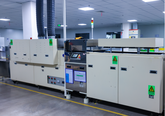
For simple electronic products, a standard SMT process may be sufficient. More complex products may require SMT, THT, mixed technology assembly, X-ray inspection, electrical testing, functional testing, programming, and other specialized processes.
Selecting an experienced PCB assembly manufacturer can help improve manufacturing quality, reduce production risks, control costs, and shorten time to market.
With capabilities covering PCB manufacturing, PCB prototyping, quick-turn PCB production, component sourcing, SMT assembly, THT assembly, inspection, testing, and production support, Kingda provides comprehensive PCB and PCBA solutions to help customers move from design verification to small-batch production and full-scale manufacturing.