PCB Plated Hole Copper Thickness: A Practical Review for Manufacturing Teams Why Does PCB Plated Hole Copper Thickness Matter? A PCB may pass electrical testing and still fail during actual operation. One of the less obvious causes is insufficient copper thickness inside plated through-holes. Plated holes are critical electrical…
IPC Class 2 PCB Class 3 PCB: What Matters on the Production Line What Are IPC Class 2 and Class 3 PCBs? IPC PCB classifications are used to define different levels of performance, reliability, and acceptance requirements for electronic products. The same discipline applies to IPC Class 2 PCB, where…
What Is a Pseudo 8-Layer PCB? Structure, Purpose, and Manufacturing What Is a Pseudo 8-Layer PCB? PCB layer count is normally determined by the number of conductive circuit layers. For example, a conventional 4-layer PCB has four copper circuit layers, while a 6-layer PCB has six. However, the physical stackup…
PCB Design Review/PCBA Design Review Checklist: Key Process and Quality Checks Why Is PCB/PCBA Design Review Important? A successful electronic product starts with good design practices. However, even a technically correct schematic and PCB layout can create manufacturing problems if the design is not reviewed from a production perspective.…
Single-Layer vs. Double-Sided vs. Multilayer FPC: A Factory-Floor Review What Is an FPC? An FPC (Flexible Printed Circuit), also known as a flex PCB or flexible circuit, is a type of printed circuit board manufactured on a flexible insulating substrate. Unlike conventional rigid PCBs, FPCs are thin, lightweight, and capable…
PCB Panelization: 10 Critical Design and Manufacturing Why Is PCB Panelization Necessary? PCB Panelization is the process of combining multiple individual circuit boards into a larger manufacturing panel. Instead of fabricating and assembling each small PCB separately, manufacturers process several boards together and separate them after fabrication or assembly. Panelization…
PCB Right-Angle Routing: Three Reasons to Avoid 90° Traces Can PCB Traces Be Routed at 90°? When engineers first learn PCB layout, one of the most common rules is to avoid 90° trace corners. However, PCB right-angle routing is not always prohibited. Whether it should be avoided depends largely on…
What Is AOI Inspection in PCB Assembly? AOI Inspection, or Automated Optical Inspection, is an important quality-control method widely used in electronics manufacturing and PCB assembly. AOI systems use cameras to capture detailed images of a PCB assembly and compare the actual board against predefined design or inspection criteria. Depending…
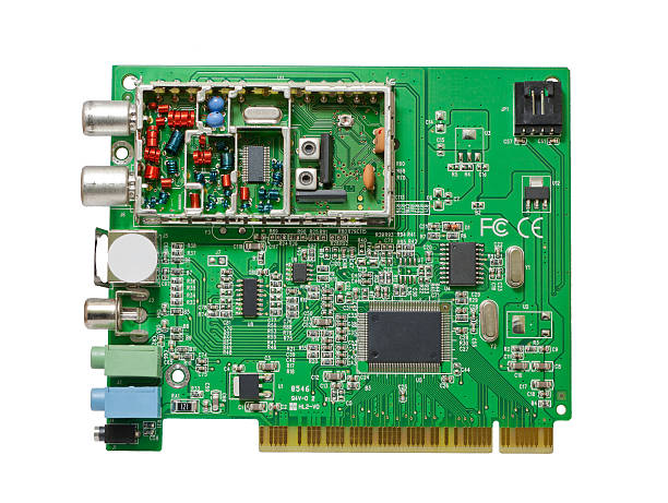
PCB Gold Fingers: Design and Assembly Considerations The row of gold-colored conductive contacts found on computer memory modules, graphics cards, and other expansion boards is commonly known as a “gold finger.” The same discipline applies to PCB Gold Fingers, where a small process drift turns into a large yield loss.…
PCB Hole Design and Slot Design Guide: Process Details and Inspection Points PCB holes and slots may look like simple features, but they play critical roles in electrical connections, component mounting, mechanical assembly, and board fabrication. A small mistake in defining a hole or slot can cause unexpected manufacturing results,…