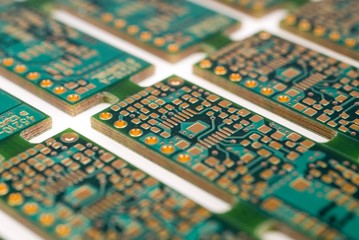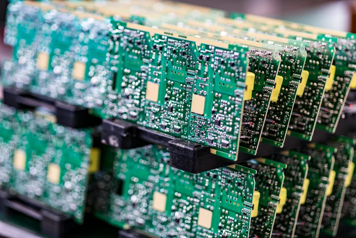

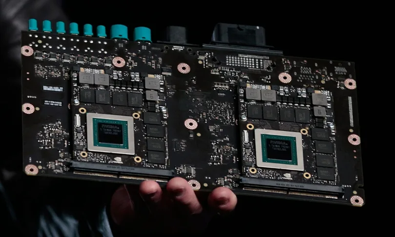
How to Fix the PCB manufacturing Too Large Error in Altium: Process Details and Inspection Points When using Altium Designer to export Gerber files, you may occasionally receive an error indicating that the PCB file is too large to be exported. The same discipline applies to PCB manufacturing, where…
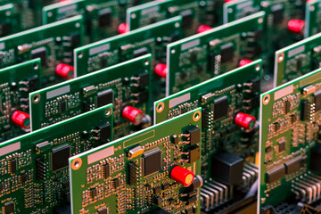
Why PCB Drill Files and Drill Drawings Matter When preparing manufacturing files for PCB fabrication, designers often focus on copper layers, solder mask, silkscreen, and board outlines while overlooking drilling documentation. However, a complete manufacturing package should clearly define both the PCB drill files and PCB drill drawing whenever…
FPC Panelization Design Guidelines FPC panelization is an important part of flexible circuit manufacturing. Because flexible printed circuits often have irregular shapes, an unsuitable panel layout can reduce material utilization, increase manufacturing difficulty, and raise production costs. The same discipline applies to FPC Panelization, where a small process drift…
What Are PCB Countersunk Holes? PCB countersunk holes are specially machined holes designed to allow the head of a screw or bolt to sit flush with, or below, the surface of a printed circuit board. This structure is useful when a PCB must maintain a low-profile surface or when…
PCB Back Drilling: How It Improves High-Speed Signal Integrity As digital systems continue to operate at higher data rates and frequencies, maintaining signal integrity has become a critical requirement in modern PCB design. Conventional through-hole vias can introduce unwanted electrical structures that negatively affect high-speed signal transmission. One effective…
BGA PCB Surface Finish Risks and How to Prevent Soldering Defects As electronic products continue to become smaller, thinner, and more powerful, BGA assembly has become increasingly common in high-density electronic devices. Ball Grid Array (BGA) packages place solder balls underneath the component body, allowing a large number of…
How to Do PCB Panelization for SMT Assembly In modern electronics manufacturing, PCB Panelization is widely used to improve production efficiency, simplify handling, and reduce manufacturing costs. Instead of processing individual circuit boards one at a time, multiple PCB units are arranged into a larger manufacturing panel and processed…
PCB Panelization for SMT Assembly: Complete Design Guide In modern electronics manufacturing, PCB panelization is widely used to improve production efficiency, reduce handling time, and optimize manufacturing costs. Instead of processing every individual printed circuit board separately, multiple PCB units can be combined into a larger manufacturing panel and…
How to FPC pad adhesion Lift-Off: Design, Process, and Quality Notes FPC pads provide the electrical and mechanical interface between a flexible circuit and electronic components or external wires. However, because an FPC uses a thin and flexible substrate, its copper pads can be more vulnerable to peeling than…
PCB Via vs. Pad: Differences, Hole Tolerances, and Design Guidelines When designing a printed circuit board, understanding the difference between a PCB Via and a PCB Pad is essential for achieving reliable electrical performance and smooth manufacturing. Although both can contain holes and connect to copper features, they serve…