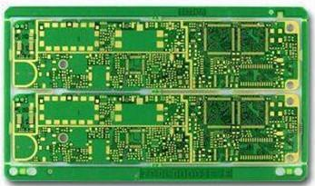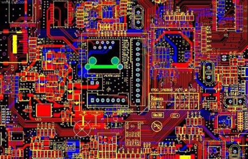
The correct installation and placement of electronic components on a PCB is one of the most important factors affecting soldering quality, assembly efficiency, and product reliability. A well-designed PCB Component Placement strategy can significantly reduce manufacturing defects, improve electrical performance, and enhance the overall reliability of electronic products.
With the continuous development of electronic devices toward miniaturization, higher integration, and faster signal transmission, modern PCB Design requires more precise component arrangement and layout planning. Improper component placement may lead to soldering problems, thermal imbalance, signal interference, mechanical stress, and difficulties during automated assembly.
During PCB manufacturing, components should be placed away from areas with large mechanical stress or excessive bending forces. The distribution of components should be as uniform as possible to avoid uneven weight distribution and PCB deformation.
Especially for large components or components with high thermal capacity, designers should carefully consider PCB size, material characteristics, and assembly conditions to prevent warping during soldering processes such as reflow soldering.
A professional PCB Layout design not only improves production efficiency but also directly affects the long-term reliability of the final electronic product.
Kingda applies advanced PCB engineering standards and manufacturing experience to optimize PCB Design processes, ensuring high-quality products with excellent assembly performance and reliability.
Basic Requirements for PCB Component Placement
A reasonable Component Layout should consider manufacturing processes, mechanical requirements, electrical performance, and maintenance convenience. Before starting PCB routing, engineers need to analyze component positions carefully and establish an optimized layout structure.
The main principles of component placement include:
- Avoid placing sensitive components in high-stress areas
- Maintain sufficient spacing between components
- Consider heat dissipation requirements
- Support automated SMT assembly processes
- Reduce signal interference and improve Signal Integrity
- Ensure convenient inspection and maintenance
By following these principles, manufacturers can reduce production risks and improve PCB Reliability.
Avoid Placing Components Near PCB Edges
Components located too close to the edge of a PCB may experience mechanical stress during manufacturing, assembly, transportation, or final installation.
The following problems may occur:
- Component damage during PCB handling
- Cracking of solder joints
- Damage to plated through holes
- Stress concentration around solder pads
Therefore, components should generally maintain a safe distance from:
- PCB edges
- Panel cutting areas
- Fixture clamping areas
- Mechanical mounting points
For most automated assembly processes, components should avoid being placed within approximately 5 mm of the PCB edge unless special design requirements exist.
When components must be placed near the PCB edge, the longer side of the component should be arranged parallel to the PCB edge. This helps reduce mechanical stress during PCB separation and assembly.
Large components, connectors, and ceramic capacitors near PCB edges require special attention because thermal cycling and mechanical vibration may cause solder joint fatigue over time.
Component Placement Around Large Components
Large components require sufficient surrounding space for assembly equipment, inspection tools, and maintenance operations.
During SMT Assembly, large components may affect:
- Solder paste printing
- Component placement accuracy
- Reflow temperature distribution
- Inspection accessibility
Therefore, designers should reserve enough clearance around large components to allow equipment nozzles, inspection cameras, and repair tools to operate effectively.
When placing smaller components near large components, designers should consider:
- Heat transfer effects
- Shadowing during soldering
- Accessibility for rework
- Mechanical interference
A balanced component arrangement improves both production efficiency and product reliability.
Avoid High-Stress Areas for Critical Components
Important components such as connectors, sockets, mounting holes, switches, and mechanical fixing points often experience higher mechanical stress.
Areas near:
- Screw holes
- PCB corners
- Slots
- Panel openings
- Connector interfaces
may experience increased stress concentration.
Placing sensitive or high-value components in these areas may result in:
- Solder joint cracks
- Component failure
- Reduced product lifetime
For reliable PCB Reliability, designers should keep critical components away from mechanical stress zones whenever possible.
PCB Layout Design Process
The complete PCB Layout and routing process usually includes several important stages:
- Schematic design
- Component library creation
- Design preparation
- Functional block division
- Component placement
- Placement verification
- PCB routing
- Final design inspection
During each stage, engineers must carefully review design requirements. If problems are discovered during routing or manufacturing analysis, the design should return to previous stages for correction.
A well-organized design process helps prevent costly modifications during production.
High-Speed PCB Component Placement Considerations
For high-speed circuits, component placement becomes even more critical because improper layout can negatively affect signal performance.
In high-speed PCB Design, engineers must consider:
- Signal transmission paths
- Return current paths
- Impedance control
- Crosstalk reduction
- Electromagnetic interference (EMI)
High-frequency components should be placed as close as possible to each other to minimize trace length and signal loss.
For RF applications, PCB layer structure is also very important. A typical RF PCB may use a four-layer structure, where the second layer is often designed as a continuous ground plane.
A complete ground plane helps:
- Reduce electromagnetic interference
- Improve signal stability
- Provide better return paths
- Enhance Signal Integrity
After confirming the layer structure, engineers can determine routing width, spacing requirements, and impedance control parameters.
Component Placement and SMT Manufacturing
Modern electronic products rely heavily on automated SMT Assembly technology. Therefore, component placement must consider manufacturing equipment capabilities.
Good SMT-friendly layout design should include:
- Consistent component orientation
- Proper spacing between components
- Clear polarity markings
- Standardized package placement
- Sufficient inspection space
Poor component arrangement may cause:
- Pick-and-place machine errors
- Uneven soldering
- Inspection difficulties
- Increased manufacturing costs
Optimizing PCB Component Placement at the design stage helps manufacturers achieve higher production efficiency and lower defect rates.
Improving Reliability Through Optimized PCB Layout
A reliable PCB Layout requires cooperation between electrical design and manufacturing requirements.
Engineers should consider:
Thermal Management
Components generating high heat should be positioned with proper spacing and thermal paths to prevent overheating.
Power Distribution
Power components should be placed close to related circuits to minimize voltage drop and improve stability.
Signal Routing
High-speed signal components should be arranged to minimize unnecessary routing distance and reduce interference.
Mechanical Design
Component locations should consider product assembly methods and environmental conditions.
Through careful planning, designers can improve both manufacturing performance and product durability.
Conclusion
Proper PCB Component Placement is a fundamental step in achieving reliable electronic products. A well-planned PCB Layout can reduce soldering defects, improve assembly efficiency, enhance signal performance, and increase product lifetime.
As PCB technology continues to advance toward higher speed, higher density, and smaller form factors, professional PCB Design methods become increasingly important.
By combining advanced engineering practices, manufacturing experience, and strict quality control, Kingda helps customers develop reliable and high-performance PCB solutions for applications including communication equipment, industrial electronics, automotive systems, and consumer devices.