PCB Design vs PCBA: What the Difference Means for a Build
Ask two engineers what the difference is between PCB design and PCBA and the answers will often describe the same object from different ends of the process. One is a bare board with copper, mask and silkscreen. The other is that board after components have been soldered onto it and tested. The distinction matters because the two stages have different deliverables, different failure modes and different people responsible for them.
What a Bare Board Contains
Fabrication turns a design database into a physical substrate. The PCB design and fabrication boundary sits here, where the artwork becomes laminate, copper traces and planes formed by etching, plated through holes and vias that connect layers, a solder mask that protects the copper and defines the pads, and silkscreen for identification. If the design calls for a surface finish, that is applied at the end of fabrication: hot air solder levelling, electroless nickel immersion gold or an organic coating, each with different flatness and shelf life.
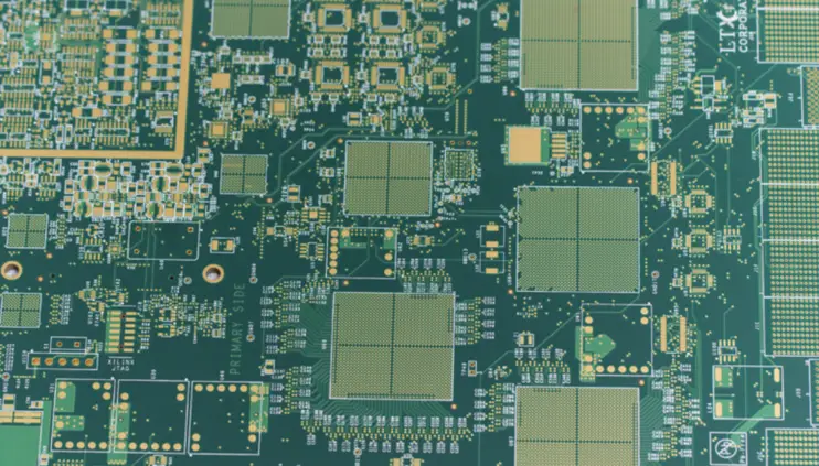
A bare board is complete in itself and can be stored, inspected and shipped. Its quality is measured by the fabricator in the language of the process: layer registration, drill accuracy, copper thickness, impedance coupons, annular ring and cleanliness. Nothing about the board at this stage knows what components will eventually be attached to it.
What PCBA Adds
PCBA stands for printed circuit board assembly, and it describes the board after components have been placed and soldered. The term covers the whole second half of the process: solder paste printing, component placement, reflow, the insertion and wave soldering of through-hole parts, cleaning where required, inspection and test. A PCBA is a functional module; a bare board is not.
This is why the two stages need separate drawings. The fabricator needs Gerber data, drill files and a stackup. The assembler needs the BOM, the pick-and-place data with rotations, a paste layer or stencil drawing, and an assembly drawing that identifies polarity and orientation. Sending the wrong package to the wrong supplier is one of the most common causes of a delayed build.
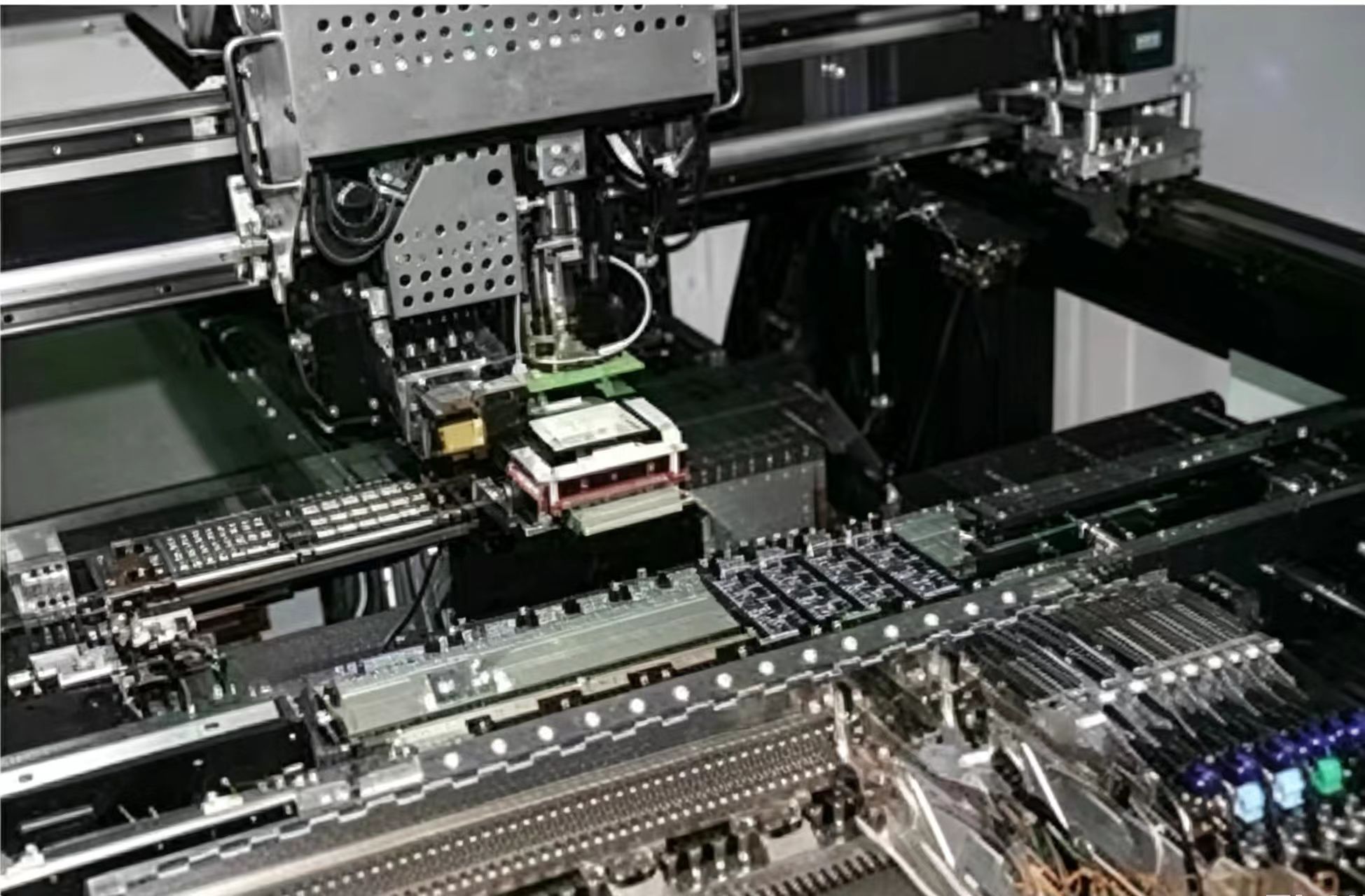
Within assembly, two technologies coexist, and the mix on a given board determines the equipment and the sequence of operations. Most modern products are predominantly surface mount with a small number of through-hole parts for connectors or power components.
Surface Mount Technology and Reflow Soldering
Surface mount technology attaches components directly to pads on the board surface. The process begins with a stainless steel stencil that prints solder paste onto the pads, followed by a placement machine that positions parts at high speed and with sub-millimetre accuracy. The board then passes through a reflow oven whose temperature profile melts the paste, forms the joints and cools them under controlled conditions.
Every parameter in that chain has a design counterpart. Pad geometry determines paste volume, paste volume determines joint shape, and joint shape determines reliability. A pad that is too large for the part produces excessive paste and tombstoning on small passives; a pad that is too small produces weak joints and opens after thermal cycling. The practical rule is to follow the manufacturer footprint recommendation rather than scaling pads to make routing easier.
Through-Hole Assembly and Mixed Technology
Through-hole components are inserted into drilled holes and soldered, usually by wave soldering or selective soldering. They are still preferred for connectors that take mechanical load, for parts that dissipate significant power and for components that must be reworked in the field. On a mixed-technology board the sequence matters: surface mount parts are reflowed first, then the through-hole parts are inserted and soldered, because the wave process would otherwise disturb the printed paste.
The design consequences are practical. Through-hole pads need sufficient annular ring and thermal relief so the solder can flow without the plane acting as a heatsink. Pin-in-paste designs, where through-hole parts are placed into paste and reflowed with the surface mount parts, can remove the second soldering operation, but they need larger paste volumes and careful stencil design.
Design Decisions That Decide Assembly Yield
Most assembly defects are designed in, not built in. Fiducials give the placement machine a reference, and they must be on the same side as the parts they locate, with clear space around them. Panelisation and breakaway tabs determine how the board travels through the line, while tooling holes and edge clearance give the conveyor something to hold.
Component orientation is equally important. All polarised parts should face the same direction where the schematic allows it, because that reduces placement programming and inspection effort. Thermal relief on ground-connected pads keeps soldering practical, and correct placement order and pad positioning prevents shadowing in the reflow oven. None of these decisions affect electrical function, and all of them affect yield.
Beyond the physical design, the handoff between design and manufacturing is a documentation problem. Each stage consumes a specific set of files, and a missing file is indistinguishable from a design error at the factory.
Documentation: What Each Stage Needs
Fabrication needs Gerber or ODB++ data, the drill file, the stackup with impedance requirements, and a fabrication drawing describing finishes and tolerances. Assembly needs the BOM with manufacturer part numbers, the pick-and-place file, the stencil or paste data, and an assembly drawing. Test needs a net list, a test point list and, for complex boards, a boundary scan description. All of it should be versioned together with the rest of the PCBA development process documents, so a change in one place does not leave another file stale.
Inspection, Test and First Article
After soldering, boards are inspected optically and, where ball grid arrays or other hidden joints are present, with X-ray. Automated optical inspection catches missing, misaligned and tombstoned parts; X-ray reveals voids, bridging and insufficient solder under area array packages. Electrical test then confirms that the assembled board actually functions, either in circuit or as a complete unit.
First article inspection is the point where design and process are reconciled. Dimensional checks, joint cross-sections and a functional run on a small number of boards provide the evidence that the design can be built repeatedly. Problems found here are corrected in the design files, not by adjusting the line.
Where the Cost Sits
Fabrication cost is driven by layer count, board area, minimum feature size, surface finish and the number of drill operations. Assembly cost is driven by the number of placement points, the number of unique part numbers, the mix of surface mount and through-hole parts, and the test strategy. Reducing part variety and keeping the finest geometry confined to the area that genuinely needs it are the two most effective ways to control the total.
FAQ
Can I order a PCBA without designing the bare board myself? You can, but the assembly house still needs fabrication data plus the BOM and placement files. If the bare board is sourced elsewhere, its stackup and surface finish must be compatible with the assembly process.
Is PCBA always more expensive than a bare board? Per unit, yes, because it includes components, assembly labour and test. The ratio depends heavily on component cost, which for a dense digital board can dwarf the fabrication price.
Why does my assembly house ask for a paste layer when I only sent Gerbers? The stencil is cut from the paste layer, and Gerber copper data alone does not contain solder paste apertures. Supplying the paste layer or the original CAD data avoids the stencil being guessed.