PCB Design Workflow: Requirements, Placement and Prototyping
A board design that goes smoothly is usually one where the early steps were taken in the right order. Requirements, the system design, the component choices and the schematic all constrain what the layout can achieve, and a layout that starts before those decisions are settled will be redone. The sequence below is the one that costs the least to follow.
Defining the Requirements
The first step is to write down what the product has to do, and to separate the must-haves from the nice-to-haves. The primary functions have to be defined before anything else, because they set the interfaces, the power architecture and the board area. Secondary functions can be added later if space and budget allow, but they must not compromise the primary behaviour of the product.
The mechanical envelope belongs in the same document. Board size, mounting positions, connector locations and height limits are constraints that the layout cannot negotiate, and putting them in writing early is what prevents a redesign in the last week.
Hardware System Design
The system design translates the requirement into blocks: how the product is powered, what it senses, how it communicates, how the user interacts with it, and what interfaces are reserved for future use. A block diagram is the natural output, and it should show the connections between the blocks rather than the details inside them.
This diagram is also the document that placement will follow. Getting the signal paths right at this stage, so that the blocks are arranged in the order the data travels, makes the layout considerably easier to complete.
Component Selection
Part selection is a balance of function, price and availability. The electrical parameters set the shortlist, and availability narrows it further, because a part that cannot be bought in production is not a candidate no matter how suitable it is. Package, temperature range, supply voltage and second-source options all belong in the comparison.
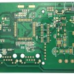
<img src="https://www.gopcba.com/wp-content/uploads/2026/08/2-2.png" alt="PCB design workflow from requirements through layout to prototype” />
Availability deserves particular attention now that lead times can move quickly. A design that depends on a single source with a long lead time is a schedule risk, and it is worth knowing before the schematic is finished rather than after the first production order.
Schematic Capture
The schematic records the nets, the reference designators and the power architecture. Beyond that, it is the place to record design intent that the layout will need: which nets carry high current, which need controlled impedance, which are length-matched, and which are sensitive.
A netlist exported without that information forces the layout engineer to infer it, and inference is where most of the avoidable iterations begin. Writing the intent down takes minutes and saves days.
Which CAD Tool and Which Outputs
Any competent layout package will produce the data a fabricator needs, so the choice is usually made on library availability, team familiarity and the constraint management the tool provides. What matters more than the tool is the discipline of keeping the design rules in the tool rather than in someone’s head, so that a violation is flagged automatically rather than caught in review.
The outputs are standard: copper layers, mask and silkscreen, drill data with tool sizes, the outline on a dedicated layer, and a fabrication drawing with the stackup and the finish.
Layout and Review
The layout follows the block diagram. Placement comes first, then the planes, then the critical routing, then everything else. Each stage should be reviewed against the original requirements rather than against the previous revision, because the requirements are what the product will be judged on.

The review before release should confirm that the design rules pass, that the fabrication drawing matches the artwork, and that every net identified as critical in the schematic has been treated as critical in the layout.
Prototyping
A prototype answers the questions the design could not: whether the impedance was what the calculation said, whether the thermal path works at load, and whether the assembly process can place the parts reliably. The prototype should use the production stackup and the production finish wherever possible, because a board built on different material verifies less than it appears to.
Building more than one panel is worth the marginal cost, because a failure on a single sample is ambiguous while the same failure on three samples is a design problem.
Assembly, Test and Debug
Assembly is where the layout decisions become visible. Courtyard clearances, part orientation and thermal reliefs all determine whether the first build goes together cleanly. Test access designed into the board makes the debugging phase far shorter, especially on the rails and on any interface that will be brought up incrementally.
Expect the first build to need a modification. Leaving a few spare pads, a zero-ohm link position and a test point on the critical nets costs nothing and can rescue a design that would otherwise need a respin. PCBA development process covers the sequence from stencil to functional test.
What the Sequence Is Really For
Why requirement definition Carries the Most Weight
requirement definition is the step where a project is easiest to influence and hardest to correct later. A board area that is 10 mm too small, a connector that has to move to the other edge, or a supply voltage that is not available from the chosen regulator are all cheap to fix in a document and expensive to fix in copper. The requirement document does not have to be long, but it has to be specific about the four things the layout will be held to: size, interfaces, power and environment.
It is also worth recording what is deliberately excluded. A product that does not need a display, a battery or a radio is one that does not need the space, the thermal path or the antenna keepout for them, and saying so prevents a later reviewer from adding them back as though they had been forgotten.
Keeping the Documents in Step
Once the requirement, the block diagram, the schematic and the layout exist, they have a tendency to drift apart. A change made in the layout to accommodate a mechanical interference is not reflected in the schematic; a part substitution made for availability never reaches the assembly drawing. The drift is small individually and cumulative in effect.
The remedy is a single revision number that applies to the whole design, and a habit of updating every document at the same time rather than the one that is currently open. At the end of a project the difference between a clean handover and a difficult one is usually whether that habit was kept.
The value of the sequence is not the paperwork but the ordering of decisions. Requirements before design, design before selection, selection before layout, and layout before fabrication means each step has the information it needs, and no step has to be repeated because a later one changed an earlier assumption. PCB design and fabrication working together describes the last of those interfaces, and Multilayer PCB prototype requirements lists what the first build needs from the design team.
FAQ
When should the mechanical constraints be fixed? Before layout starts. Board outline, mounting positions, connector locations and height limits all constrain the placement, and moving them afterwards invalidates the layout.
How do I choose components for a small production run? By availability first, then by the electrical parameters that the design cannot compromise. A part with a long lead time or a single source is a risk that has to be weighed against its advantages.
How many prototypes should be built? More than one. Three boards distinguish a design problem from a manufacturing hiccup, and the marginal cost is small compared with a respin.