Edge Clearance: Key Checks Before Release
PCB edge clearance is the distance between the board profile and the nearest copper, component or hole. The profile is a machined surface, so it has a tolerance that is much wider than the artwork tolerance, and the features near it have to be placed with that tolerance in mind. A design that ignores the rule produces boards with exposed copper on the edge, a short to a housing, or a component that is cut by the router.
Why Edge Clearance Matters
The board profile is routed, milled or scored, and the routing process has a tolerance of a few tenths of a millimetre. The copper has to stay inside the profile even at the extreme of those tolerances.
An exposed copper edge is a corrosion site and a potential short against a metal housing or a conductive gasket. It is also a place where the plating solution can collect and dry.
The laminate itself also needs protection, because the resin at the edge is exposed and absorbs moisture faster than the surface. An edge that is too close to copper has less material to insulate it.
The rule also protects the components, since a part that overhangs the profile can be hit by the router or by the depanelisation tool.
Copper Pullback from the Edge
The usual pullback for copper on an outer layer is between 0.2 and 0.5 mm, and the value depends on the profile tolerance and on the process that cuts the board.
A plated edge or a castellated edge is the exception, since the copper is deliberately wrapped over the profile. Those features need special process control and a larger clearance elsewhere on the same edge.
The pullback applies to planes as well as to traces, so a ground pour has to be pulled back by the same distance or more. A pour that runs to the edge is a common source of an exposed copper defect.
The outline tolerance is the number that the pullback is derived from, so the two should be specified together rather than independently.
Component Clearance and Overhang
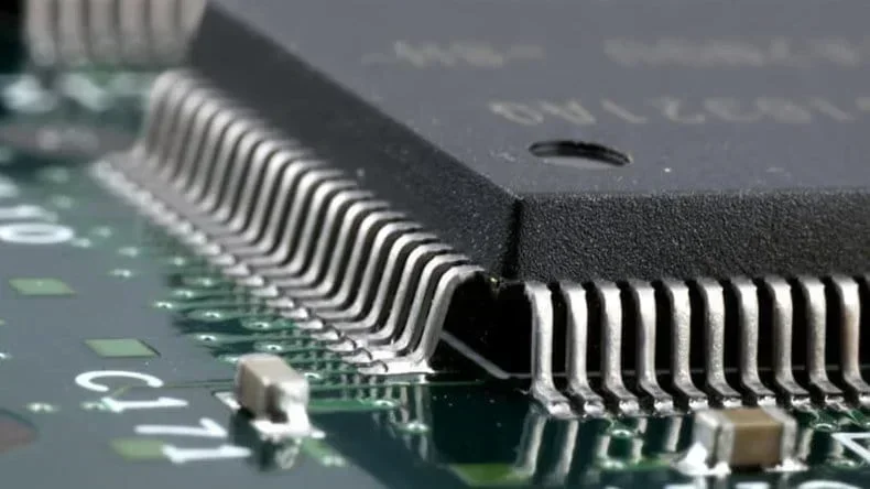
A component should not overhang the profile, with the exception of a connector that is designed to, such as a card edge or a board to board part with a housing overhang.
The clearance for a component is larger than for copper, because the body has height and the router can catch it. A few millimetres is typical, and more where the part is tall or fragile.
The courtyard convention covers the body but not the tooling, so the nozzle that places the part and the nozzle that reworks it both need space that the courtyard may not show.
A connector that overhangs deliberately should be shown on the mechanical drawing, and the panel layout has to keep the rail clear of the overhang.
Holes, Vias and the Edge
A hole near the profile has less laminate around it, and a drill that breaks through the edge leaves a semicircular feature that is not plated correctly.
The clearance for a hole is measured from the edge of the hole rather than from its centre, and it is usually larger than the copper pullback because the drill has its own tolerance.
A via near the edge is also close to the router, so the same rule applies and the pad should be included in the measurement.
A mounting hole that is intended to be at the edge is a design decision and should be dimensioned from the profile with its own tolerance rather than left to the general rule.
Panel Rails and Breakaway Areas
The panel rail and the breakaway tab are cut after assembly, so the copper and the components near a tab see the highest mechanical stress in the whole process.
The tab area should be kept clear of components and of critical traces, and the clearance around a tab is usually larger than the general edge clearance.
A v-score also removes material and creates a stress concentration along its line, so the copper should be pulled back from the score line as well as from the profile.
The tab design rules and the edge clearance rules should be applied together, since a tab that is placed where the layout needs a trace is a conflict that is found only at the panel stage.
<img src="https://www.gopcba.com/wp-content/uploads/2026/08/17aa72336fa5.webp" alt="Dimension marking the clearance between a trace and the board edge” />
Routing the Edge Region
The routing of a board that sits inside a housing has to consider the housing as well as the profile, because a metal housing can short against an exposed trace even when the copper is inside the board outline.
A conductive gasket or a metal clip that touches the edge is a direct path to an exposed layer, which is why the pullback for a product in a metal enclosure is often twice the value used for a bare board.
The routing near the edge should also avoid a long parallel run to the profile, because the edge is a discontinuity and a trace that runs along it can couple to the housing or to a neighbouring board in a stack.
Where a trace has to run near the edge, it should be short and it should be on an inner layer, where the laminate provides the insulation that the surface cannot.
Verifying the Clearance
A design rule check catches the copper that violates the pullback, and the rule should be set from the profile tolerance rather than from a default value in the tool.
The component clearance is not caught by the copper rule, so the placement should be checked against the outline separately, ideally with a keep out region drawn on the mechanical layer.
The first article inspection should include the edge, and it should look for exposed copper, a burr and a component that is close to the profile. A photograph of the edge is a useful record.
A useful practice is to draw the profile at the minimum and the maximum of its tolerance on the mechanical layer, and to check the layout against both. The difference between the two shows immediately whether the margin is real or assumed.
A board that passes the design rule check can still fail at the edge, because the rule uses the nominal outline rather than the profile that the router actually cuts.
Practical Rules
Specify the profile tolerance first, then derive the copper pullback from it rather than choosing a number by habit.
Pull back every layer, including the planes, and check the pour on the outer layers after the polygon is regenerated.
Keep the components clear of the profile and the tab area, and check the height as well as the footprint.
Record the clearance rules in the fabrication notes, and inspect the edge on the first article with the quality check.
FAQ
What is a typical copper pullback from the board edge? Between 0.2 and 0.5 mm on an outer layer, depending on the profile tolerance and on the process that cuts the board.
Can a component overhang the board edge? Only by design, such as a connector with a housing overhang. In that case the overhang is shown on the mechanical drawing and the panel rail is kept clear.
Why does a tab area need more clearance? Because the tab is broken after assembly and the force is applied to the laminate around it. Copper and components near a tab see the highest stress.