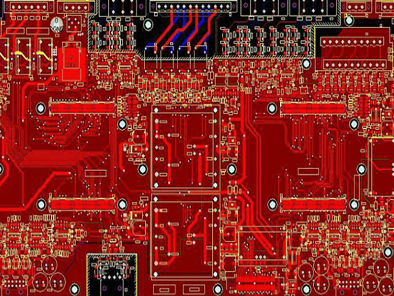
PCB Electrical Clearance and Spacing Requirements Explained
Spacing is the part of a layout that nobody notices until the board fails. A trace that runs 4 mil from its neighbour is a reliability experiment, not a design; a pad that sits 0.1 mm from the board edge is a short waiting to happen after depanelisation. This article separates the spacing rules into the two families that a layout engineer actually needs to track and gives the practical numbers for each.
Two Families of Spacing Rule
Electrical clearance covers the distance needed to withstand a voltage without breakdown, tracking or arcing. It is set by the applied voltage, the pollution degree of the environment and the coating, if any, that protects the surface. Non-electrical spacing covers everything needed for the board to be manufactured and assembled: solder mask webbing between pads, silkscreen legibility, keep-outs for the router and clearance for assembly tooling.
The two families are usually checked by different people. A design rule check in the layout tool handles the manufacturing side well if the rule file is accurate. The electrical side needs a deliberate review against the safety standard that applies to the product, because it depends on the working voltage rather than on the process capability of the fabricator.
Trace to Trace Spacing
The minimum trace spacing a fabricator can hold depends on the copper thickness and the etching process. On one ounce copper with standard subtractive etching, 4 mil is a common floor and 10 mil is comfortable; finer spacing is possible on half ounce copper and gets progressively harder as copper weight rises. Wider spacing costs nothing but board area at the layout stage, so wherever the routing allows, use more than the minimum. The distance a via must keep from an unrelated trace on the same layer is often larger than the trace to trace rule, and is covered with the notes on via to trace clearance in multilayer boards.
Spacing also sets crosstalk, which is why the electrical and manufacturing numbers are not the only ones that matter. Bringing an aggressor trace closer to its neighbour raises the coupled noise roughly in proportion to the reduction in gap, so a parallel run that is acceptable at 10 mil can be marginal at 4 mil over the same distance. Where the two rules disagree, the signal integrity requirement wins, and the routing should be rearranged rather than pushed to the process limit.
Hole Size and Pad Width
The smallest finished hole is a process question. Mechanically drilled holes normally start at 0.20 mm, while laser drilled microvias can go much smaller, commonly 4 mil and below. Hole diameter tolerance is typically held to within 0.05 mm and varies a little with the laminate. The pad around the hole has to leave an annular ring wide enough to survive drill registration error, so the minimum pad width, measured across the pad, should not fall below the hole diameter plus twice the required ring.
Pad to Pad Spacing
Adjacent pads need a pad spacing that still leaves a solder mask web between them. If the gap is too small, the mask cannot adhere and will lift or be washed away during development, which exposes bare copper between two pads and invites bridging during reflow. A common rule is at least 0.2 mm between separate pad features, with the solder mask web checked separately because the mask dam is narrower than the copper gap by the mask registration tolerance on each side.
Fine pitch packages make this rule painful. Below roughly 0.4 mm pitch there is no room for a mask web at all, so the mask is defined as a single opening covering the whole pad row and the paste stencil aperture and pad geometry take over the job of separating the joints. The layout still has to respect the fabricator limit on pad spacing, which is why the land pattern is normally taken from the manufacturer recommendation rather than scaled down further.
Copper to Board Edge
The copper to edge rule exists for two reasons: the router can chip the laminate and expose copper, and outer layer copper that reaches the edge can short against a metal enclosure or an adjacent panel. A practical figure is 0.3 mm from any current carrying copper to the finished outline. Large copper pours are usually pulled back further, often 20 mil, so that the pour is not exposed by normal routing tolerances.

The edge clearance rule is usually implemented with a keep-out layer that the pour obeys automatically, rather than by shaping each polygon by hand. That way a later change to the outline does not silently push copper onto the edge. Tooling and breakout areas along the panel rail need their own keep-out, separate from the finished board outline.
Solder Mask and Silkscreen Limits
Silkscreen has a legibility floor as well as a spacing rule. Characters below about 0.8 mm in height, or with strokes under 0.15 mm, tend to blur or smear during printing, so most fabricators quote a minimum line width and height below which they will not guarantee clear text. Legend must also stay off the pads. A solder mask dam that runs across a pad opening will not print, and legend ink on a pad prevents solder wetting and interferes with placement.
The usual requirement is 8 mil between the legend edge and the pad opening, relaxed to about 4 mil on dense assemblies where the fabricator can clip the legend automatically. Clipping is a repair, not a design intent, so it is better to place the reference designators where they fit cleanly. Pad and land pattern dimensions are described further in the notes on PCB pad design standards.
Creepage and Voltage Driven Rules
Above roughly 50 V, the electrical rule begins to dominate the layout. Creepage, the distance along the surface of the insulator between two conductive parts, has to increase with voltage, with pollution degree and with altitude, because the surface can collect dust and moisture that reduce the effective withstand distance. Clearance, the distance through air, follows a similar table. Coating the assembly with conformal coating reduces the required creepage but does not remove the requirement to check it.
On mains connected and industrial products, the numbers come from the applicable safety standard rather than from the fabricator capability sheet, and the layout should be reviewed against that standard with the working voltage of each net clearly defined. A common mistake is to apply the mains rule only to the primary circuit while forgetting the isolated secondary side, which can still carry a high potential relative to earth.
Mechanical and 3D Clearance
Finally, components must clear each other in three dimensions as well as two. Height matters above the board, where a tall capacitor can meet the inside of an enclosure, and below it, where a through-hole lead can touch a mounting boss. Boards that plug into a chassis need clearance for the guide rails along the edges, which normally sets a component free band wider than the electrical edge rule. The notes on board outline and mounting design cover how these mechanical keep-outs are defined.
FAQ
What is the minimum trace spacing for a standard board? Four mil is a practical floor on one ounce copper, with 6 to 10 mil more comfortable. Thin copper allows finer spacing, but the cost rises quickly below 4 mil.
How much creepage do I need at 230 V? It depends on the pollution degree and the safety standard that applies. For a typical pollution degree 2 application, several millimetres are required, so the value must be taken from the standard table rather than from the fabricator rule file.
Can silkscreen be printed over a pad if the fabricator clips it? It can be clipped, but the result is unpredictable. Place legend so that it clears the pad opening by 8 mil and the clipping step never has to be used.