PCB Hole Structures: Blind Via, Buried Via and Microvia
The holes in a circuit board are not all the same thing, and the differences between them determine how dense a design can be, how much it costs and how reliable it turns out. A through hole that accepts a component lead, a via that connects two layers and a microvia that connects two adjacent layers are different structures with different fabrication processes, different reliability characteristics and different costs. Understanding the family is what allows a designer to choose the simplest one that will do the job.
The Basic Structures
A plated through hole runs from the top of the board to the bottom, and it connects every layer it passes through. It is the cheapest to make because it is drilled in one operation after lamination and plated in one pass, and it is the most reliable because the plating is a continuous barrel. Its cost is board area: the hole, its annular ring and the clearance around it occupy space on every layer, whether or not the net needs to be there.
A blind via starts on an outer layer and ends on an inner one. A buried via starts and ends on inner layers and is invisible from outside. Both remove the unused portion of the barrel, which frees routing space on the layers the via does not pass through, and both require the board to be built in stages with a lamination cycle between them.
Microvias and High Density Interconnect
A microvia is a small hole, typically under a tenth of a millimetre in diameter, formed by laser rather than by a drill and connecting two adjacent layers. It is the building block of high density interconnect, where layers are added in sequence and each addition allows another level of connections. Because the hole is shallow, the plating is more uniform and the reliability is good, provided the aspect ratio is kept within the process limit.
Stacking microvias, where one sits directly on top of another, allows the density to rise further but concentrates the stress at the interface between them, and it is the configuration that most often fails in thermal cycling. Staggering them, so that each microvia lands on a pad rather than on the one below, is more reliable and occupies more area. Our blind and buried via article describes the process steps involved.
Filled, Tented and Capped Vias
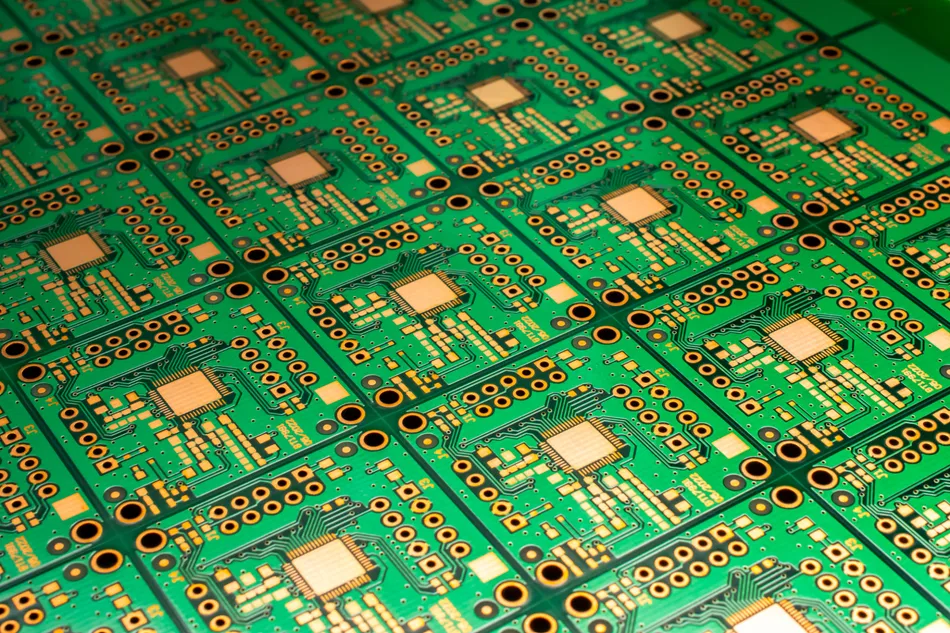
A via that is not used for a component can be left open, covered with solder mask or filled with material. Tenting, where the solder mask covers the via, prevents solder from wicking into the barrel during assembly and is standard on most boards. Filling, where the barrel is filled with a conductive or non-conductive material and then capped with copper, is used where a pad must be placed directly over the via, which is common beneath a ball grid array or a fine pitch package.
Filled and capped vias are more expensive because they add process steps, and they have their own failure mode: a filled via that is not completely filled leaves a void under the cap, and the cap can collapse during assembly. The filling material and the process control matter as much as the geometry.
Aspect Ratio and Drilling
The aspect ratio of a hole is its depth divided by its diameter. A high ratio is difficult to drill and difficult to plate, because the drill wanders and the plating solution has to exchange chemicals along a deep narrow channel. Every fabricator has a maximum ratio it can hold reliably, and a design that exceeds it will produce boards with thin or voided barrels that pass electrical test and fail later.
Mechanical drilling is used for through holes and, at small diameters, it consumes drill bits at a rate that affects cost. Laser drilling is used for microvias because a mechanical bit of that size would break, and the laser parameters have to be matched to the material, particularly for glass reinforced laminates where the glass and the resin ablate at different rates.
Selecting the Right Structure
The selection is straightforward if the question is asked in the right order. Start with through holes, which are the cheapest and most reliable. Add blind and buried vias only where the routing genuinely cannot be completed without them, and count the extra lamination cycles that each level costs. Use microvias only where the density requirement justifies the process, and avoid stacking them unless there is no alternative.
The design should also keep the aspect ratio within the fabricator’s capability rather than at its limit, and should state the finished hole size rather than the drill size, because the two differ by the plating thickness and the ambiguity is a common cause of arguments at first article. Our design release checklist places those checks in the review sequence.
Cost and Reliability Trade-Offs
The structures form a ladder of cost, and each rung buys routing space. Through holes are effectively free once the board is drilled, blind and buried vias cost an extra lamination cycle each, and microvias cost a laser process and a sequential build. The designer’s job is to climb the ladder only as far as the routing requires, because every rung adds cost, adds lead time and adds a failure mode.
Reliability follows the opposite pattern in one respect. A shallow microvia is easy to plate uniformly and is a reliable structure in isolation; the reliability risk comes from stacking them or from placing them where thermal expansion concentrates stress. A deep through hole in a thick board is the harder structure to plate well, but it is a single continuous barrel with no internal interface to fail. Our design release checklist places those considerations in the review sequence.
Verification and Inspection
Hole quality is verified by cross section. A coupon from the panel border is mounted, ground and polished, and the plating thickness is measured at the surface, the middle and the bottom of the barrel. For microvias the target is the interface between the microvia and the pad below it, because that is where a separation would begin.
Thermal stress testing, in which the coupon is floated on molten solder and then re-examined, is the traditional acceptance test and remains the most convincing evidence that the plating will survive assembly and service. Where the design uses stacked microvias, a thermal cycling test on a representative coupon is worth more than any calculation, because the failure mode depends on the interaction between the materials rather than on the geometry alone. Our component tolerance and reliability notes describe how that result feeds into the design.
FAQ
What is the difference between a via and a through hole? Physically very little; a via is a plated hole intended only to connect layers, while a through hole usually also accepts a component lead. The distinction matters for the pad and mask treatment.
Why are blind and buried vias more expensive? Because they require the board to be laminated in stages, with drilling and plating between the stages. Each additional stage consumes a press cycle and adds its own yield loss.
Are stacked microvias reliable? They can be, but they concentrate thermal cycling stress at the interface. Staggered microvias are more reliable and are preferred where the density allows.