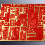
PCB Impedance Matching and Buildup Process Explained
When a signal leaves a driver it should arrive at the receiver with as little loss and as little reflection as possible. That happens only when the impedance of the trace equals the impedance of the source, which is what impedance matching means in practice. On a low-speed board the requirement is invisible. On a thick board with long traces routed through several via transitions, it becomes the constraint that decides the stackup, the materials, and the price.
What Impedance Matching Actually Requires
The characteristic impedance of a trace is not a value the designer assigns directly. It emerges from the geometry and the material: whether the trace runs on an outer layer or an inner layer, the distance to the reference plane, the trace width, the copper thickness, and the dielectric constant of the laminate. Change any one of those and the value moves. Impedance can therefore only be confirmed after routing, and two fabricators building the same design to the same drawing can deliver slightly different results unless the stackup and the process are specified identically.
Simulation tools have their own limitation. The models and the numerical methods behind them do not capture every small discontinuity: a stub, a via with an unplanned barrel, a short parallel run that widens the effective line. Where the model cannot see the discontinuity, the schematic can only compensate with a termination, such as a series resistor, that softens the effect. The real fix is to avoid the discontinuity in the layout, which means keeping the reference plane continuous, minimizing via transitions, and not changing width in the middle of a matched run.
Microstrip, Stripline and What Sets the Value
The layer a trace sits on determines which relationship applies. A microstrip is a trace on an outer layer with one reference plane below it. A stripline is buried between two reference planes, and a double stripline is offset between them. Buried traces are surrounded by dielectric on both sides, which shields them and reduces radiation, at the cost of tighter fabrication tolerance because two dielectric thicknesses now affect the result instead of one. An outer-layer trace is easier to tune after the fact and easier to probe, but it radiates and it is exposed to handling.
Because geometry and material both matter, the impedance target belongs on the fabrication drawing together with the layer it applies to, not as a single number for the whole board. The available trace geometries are compared in microstrip and stripline routing.

The Buildup Process: a n b
Thick high-density boards are usually built by sequential lamination rather than by pressing every layer at once. The sequence starts with a core board, which may be a conventional double-sided or multilayer panel or one that already contains buried and blind vias, and that core is plugged and planarized. A resin-coated copper layer is then laminated on, laser drilled, plated, and patterned, and the cycle repeats on one or both faces. The resulting structure is written as a n b, where a is the number of buildup layers on one side, n is the core, and b is the number on the other.
Each repetition adds a lamination, a laser drilling step, and a plating step, and each of those steps has a yield. That is the structural reason a dense board costs so much more than several simpler boards: the process is not merely longer, it is repeated, and the panel is at risk of scrap at every pass.
Core Boards and Plugging Before Buildup
The core is not always a plain panel. It can be a conventional multilayer board, or one that already carries buried and blind vias, and in either case it has to be plugged and its surface ground flat before anything is laminated on top. Resin filling, baking, and planarization add steps before the buildup process even starts, and each of them has to be complete before the next lamination, because material trapped under a new layer cannot be recovered afterwards.
The order of operations matters. Vias that will be covered by a subsequent layer are processed first, so that drilling and plating of the remaining holes can follow the normal route afterwards. Reversing that order produces a panel where deep holes and shallow ones are plated under different conditions. The data preparation for each of those stages is covered in HDI board CAM methods.
Rigid, Flex and Rigid-Flex Thickness
The choice of substrate changes the mechanical envelope that the rest of the product has to respect. Rigid boards are commonly built at 0.2, 0.4, 0.6, 0.8, 1.0, 1.2, 1.6, and 2.0 mm, and a mechanical engineer designing an enclosure needs those numbers early. Flexible boards are thinner, typically around 0.2 mm, and where a component has to be soldered, a stiffener of 0.2 or 0.4 mm is added behind the pad area. Rigid-flex combines both and is thicker again at the transition.
The laminates differ as well. Rigid substrates are usually paper-phenolic, paper-epoxy, glass-mat polyester, or glass-cloth epoxy; flexible substrates are typically polyester, polyimide, or fluoropolymer film. The substrate also sets the maximum temperature the assembly can see and the dimensional stability it holds, so the mechanical drawing and the fabrication drawing have to agree on which material was assumed.
Assembly Requirements on a Dense Board
On a complicated assembly, the insertion and soldering requirements are as strict as the layout rules. Through-hole parts should be prepared before insertion, with leads tinned if their solderability is in question, and formed so that the lead pitch matches the hole pitch. The forming also has to leave enough lead length to dissipate soldering heat and to give the joint its mechanical strength.
Insertion then follows an order that keeps later steps possible: low parts before tall ones, small before large, light before heavy, and ordinary parts before special ones, so that nothing already fitted blocks the next operation. Markings should face the readable direction, polarized parts must follow the drawing exactly, and the finished arrangement should be even rather than tilted, crossed, or interleaved. Every solder joint is judged on three things: mechanical strength, reliable conduction, and a smooth clean surface. Automated assembly and test on this class of board depend on routing discipline described in high-frequency trace and data bus routing.
Why Dense Prototypes Cost More
The price of a prototype is set by the number of process steps and by the panel area consumed, not by the layer count alone. A thick board needs more lamination cycles, more drilling operations, and more inspection points. It also often has to be produced alone on its own panel rather than nested with other parts, and a specialty material stocked in small quantities carries its own premium. When a prototype uses an unusual substrate, the first article also pays for qualifying the process on that material.
That is why the same function can be built on a modest stack for a fraction of the price if the design is willing to route differently. The question to ask at the start of a program is not how many layers the previous product used, but how many the signal integrity budget actually requires.
FAQ
Why can impedance only be verified after routing? Because it depends on the finished geometry: layer, width, dielectric thickness, copper weight, and laminate. The value exists only once the trace has been placed.
What does a n b mean? It describes a buildup structure: a buildup layers on one face, n for the core board, and b buildup layers on the other face.
Why is a 32-layer board so much more expensive than four 8-layer boards? Because the buildup sequence repeats lamination, laser drilling, and plating, and each repetition adds cost and a chance of scrap.
What thicknesses should I assume for a rigid board? The common set is 0.2, 0.4, 0.6, 0.8, 1.0, 1.2, 1.6, and 2.0 mm. Flex is around 0.2 mm, plus a stiffener wherever parts are soldered.