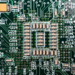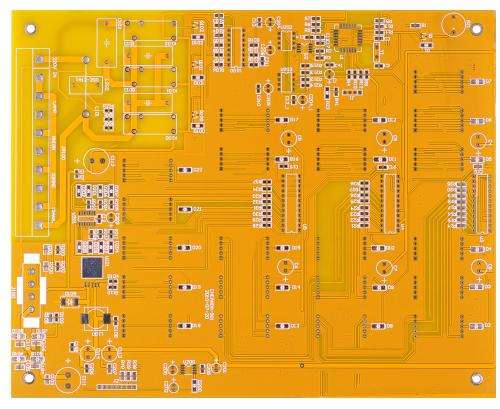
With the rapid development of electronic technology, modern electronic products are continuously evolving toward smaller sizes, higher integration levels, faster transmission speeds, and improved reliability. From smartphones and wearable devices to automotive electronics, industrial control equipment, communication systems, and intelligent hardware, almost every electronic product depends on advanced circuit board technology.
Among all PCB technologies, PCB Layout Design is one of the most critical stages that determines the electrical performance, manufacturing feasibility, and long-term reliability of electronic products.
A PCB is not only a carrier for electronic components but also a platform responsible for:
- Electrical signal transmission
- Power distribution
- Component interconnection
- Electromagnetic control
- Mechanical support
Especially for Multilayer PCB and Flexible PCB designs, engineers must carefully consider trace arrangement, layer structure, signal paths, and manufacturing limitations.
An optimized PCB Layout Design can effectively improve:
- Signal integrity
- Power integrity
- Electromagnetic compatibility
- Thermal performance
- Manufacturing yield
However, improper layout may cause:
- Signal reflection
- Crosstalk interference
- Voltage instability
- Excessive electromagnetic radiation
- Difficult PCB production
Therefore, following professional PCB layout principles is essential for developing high-performance electronic products.
As an experienced PCB manufacturer, Kingda provides professional PCB Manufacturing services, including multilayer PCB fabrication, flexible circuit production, high-speed PCB solutions, and customized PCB development support.
Basic Principles of PCB Layout Design
The purpose of PCB Layout Design is to achieve an optimized arrangement of components and conductive paths while ensuring electrical performance and manufacturing reliability.
A successful PCB layout should consider the following aspects:
Electrical Performance
The PCB design must ensure stable transmission of signals and power.
Important factors include:
- Signal path length
- Impedance control
- Return current path
- Grounding structure
- Noise suppression
For modern high-frequency electronic products, these factors directly influence product performance.
Manufacturing Capability
A PCB design must match actual PCB Manufacturing capabilities.
Designers need to consider:
- Minimum trace width
- Minimum spacing
- Via dimensions
- Copper thickness
- Layer alignment accuracy
A design that exceeds manufacturing limits may result in:
- Lower production efficiency
- Increased cost
- Reduced reliability
Therefore, close communication between PCB designers and manufacturers is important.
Reliability Requirements
A reliable PCB design should consider:
- Mechanical stress
- Thermal expansion
- Component heat distribution
- Long-term operating conditions
This is especially important for automotive electronics, medical equipment, aerospace systems, and industrial applications.
PCB Trace Spacing Design Principles
Trace spacing is one of the most important factors in PCB Layout Design.
The distance between different electrical networks depends on:
- Operating voltage
- Insulation requirements
- Manufacturing process
- Component spacing
- Environmental conditions
Proper spacing prevents electrical problems and improves PCB reliability.
Electrical Clearance and Insulation Design
When high-voltage and low-voltage circuits exist on the same PCB, sufficient clearance must be maintained.
Insufficient spacing may cause:
- Electrical breakdown
- Leakage current
- Short circuits
- Safety risks
For power supply circuits and industrial control systems, insulation design is a key requirement.
Engineers must consider:
- Voltage difference
- Material characteristics
- Safety standards
- Environmental factors
High-Density PCB Spacing Requirements
For advanced Multilayer PCB designs, more circuits must be placed into limited space.
High-density PCB layouts require:
- Fine trace spacing
- Smaller vias
- Accurate layer alignment
- Advanced manufacturing processes
Designers need to balance:
- Circuit density
- Signal performance
- Manufacturing feasibility
PCB Routing Design Principles
PCB Routing directly affects electrical performance and manufacturing quality.
A good routing strategy improves:
- Signal transmission
- Noise control
- Electromagnetic performance
- Product reliability
Avoid 90-Degree Trace Corners
Traditional PCB design recommends avoiding sharp 90-degree corners.
Sharp corners may create:
- Impedance changes
- Signal reflection
- Uneven current distribution
For better performance, designers usually use:
- 45-degree routing
- Arc routing
These methods provide smoother signal transmission.
Smooth Connection Between Traces and Pads
The connection between traces and component pads should be carefully designed.
Poor connections may create mechanical stress points.
A common improvement method is the use of teardrop structures.
Benefits include:
- Increased pad strength
- Reduced cracking risk
- Improved drilling tolerance
- Higher manufacturing reliability
This is especially useful for fine-pitch components and high-density PCB designs.
PCB Trace Width Design Guidelines
Trace width determines the current carrying capability and electrical performance of PCB circuits.
The main influencing factors include:
- Current level
- Copper thickness
- Temperature rise
- Signal frequency
Signal Trace Width
Signal traces focus on impedance control rather than simply increasing width.
Important factors include:
- Dielectric thickness
- Copper thickness
- Reference plane distance
- Signal frequency
In High-Speed PCB Design, maintaining stable impedance is essential for good Signal Integrity.
Power Trace Width
Power traces usually require greater width because they carry higher current.
Wider traces provide:
- Lower resistance
- Reduced voltage drop
- Better heat dissipation
For complex Multilayer PCB, dedicated power layers are often used instead of large surface traces.
Ground Design and Return Current Path Optimization
A proper grounding structure is one of the most important elements in PCB Layout Design. Poor grounding design can lead to:
- Signal distortion
- Increased noise
- Unstable power supply
- Electromagnetic interference problems
In high-speed circuits, return current does not always follow the shortest physical path. Instead, it follows the path with the lowest impedance, especially at high frequencies.
Therefore, engineers must carefully design:
- Ground planes
- Signal reference layers
- Ground vias
- Power distribution structures
A continuous ground plane in a Multilayer PCB can provide a stable return path and significantly improve Signal Integrity.
Power Integrity Design Principles
With the increasing power consumption of modern electronic devices, power integrity has become an essential part of High-Speed PCB Design.
A stable power distribution network should minimize:
- Voltage fluctuation
- Power noise
- Current loss
- Ground bounce
Common design methods include:
Dedicated Power and Ground Layers
In a Multilayer PCB, separate power and ground layers are often used.
Advantages include:
- Lower power impedance
- Better current distribution
- Reduced electromagnetic radiation
- Improved circuit stability
Decoupling Capacitor Placement
Decoupling capacitors should be placed as close as possible to IC power pins.
This helps:
- Reduce high-frequency noise
- Provide instant current supply
- Improve power stability
Poor capacitor placement may cause unstable operation, especially in high-speed digital circuits.
High-Speed PCB Routing Design Principles
With the rapid development of 5G communication, artificial intelligence equipment, high-performance computing, and automotive electronics, High-Speed PCB Design has become increasingly important.
High-speed signals are sensitive to PCB structures because their performance depends on:
- Trace length
- Impedance consistency
- Layer structure
- Crosstalk control
- Return path quality
Signal Integrity Control
Signal Integrity refers to the ability of a signal to maintain its original waveform during transmission.
Poor signal integrity may result in:
- Signal reflection
- Overshoot and undershoot
- Timing errors
- Data transmission failure
To improve Signal Integrity, designers should consider:
Control Signal Trace Length
Longer traces increase:
- Signal delay
- Transmission loss
- Reflection risk
High-speed signal traces should be kept as short as possible.
Maintain Controlled Impedance
For high-speed signals, impedance consistency is critical.
Factors affecting impedance include:
- Trace width
- Trace thickness
- Dielectric material
- Distance to reference plane
A proper PCB stack-up design helps maintain stable impedance.
Avoid Reference Plane Discontinuity
When high-speed signals cross gaps in reference planes, the return current path is interrupted.
This may cause:
- Increased loop area
- Higher EMI radiation
- Signal quality degradation
Therefore, high-speed routing should always maintain a continuous reference plane.
Differential Pair Routing Principles
Differential signaling is widely used in modern electronic systems because it provides strong noise resistance.
Common differential applications include:
- USB
- PCI Express
- Ethernet
- High-speed memory interfaces
Proper differential pair design requires:
Equal Trace Length
The two traces in a differential pair should maintain similar lengths.
Length mismatch may cause:
- Timing errors
- Phase differences
- Signal distortion
Engineers often apply length matching techniques to maintain signal synchronization.
Constant Trace Spacing
The spacing between differential traces should remain consistent.
Changes in spacing may affect:
- Differential impedance
- Signal balance
- Transmission quality
Reduce Unnecessary Vias
Excessive vias may introduce:
- Impedance discontinuity
- Additional signal loss
- Manufacturing complexity
For high-speed differential signals, layer transitions should be minimized.
Crosstalk Reduction in PCB Routing
Crosstalk occurs when electromagnetic energy from one trace affects another nearby trace.
It becomes more serious when:
- Signal frequency increases
- Trace spacing decreases
- Parallel routing distance increases
To reduce crosstalk in PCB Routing, designers can use several methods.
Increase Trace Spacing
Increasing the distance between signal traces reduces electromagnetic coupling.
Sensitive signals should be separated from:
- Clock signals
- High-current lines
- Switching power circuits
Use Ground Guard Traces
Ground guard traces can isolate important signals from surrounding interference.
Benefits include:
- Reduced signal coupling
- Improved noise immunity
- Better electromagnetic performance
Optimize Layer Arrangement
A proper Multilayer PCB stack-up can reduce interference by placing sensitive signals close to reference planes.
Electromagnetic Compatibility Design Principles
Electromagnetic Compatibility is a key requirement for modern PCB products.
A PCB must not only function correctly but also avoid generating excessive electromagnetic interference.
EMC problems usually come from:
- High-speed switching signals
- Poor grounding
- Large current loops
- Improper routing
Reduce Current Loop Area
Large current loops generate stronger electromagnetic radiation.
To reduce EMI:
- Keep signal paths short
- Provide nearby return paths
- Avoid unnecessary routing loops
Separate Noisy and Sensitive Circuits
Different circuit blocks should be arranged properly.
For example:
Power circuits should be separated from:
- Analog circuits
- Sensitive communication circuits
- Precision measurement circuits
This reduces interference between different functional areas.
Flexible PCB Layout Design Principles
Compared with rigid boards, Flexible PCB technology provides unique advantages for compact and complex electronic products.
Flexible circuits can bend, fold, and fit into limited spaces, making them widely used in:
- Mobile devices
- Wearable electronics
- Medical equipment
- Automotive systems
However, flexible PCB design requires special attention because the circuit experiences mechanical movement during operation.
Flexible PCB Material Selection
Common materials used for Flexible PCB include:
- Polyimide film
- Polyester film
- Flexible copper-clad materials
These materials provide:
- Excellent flexibility
- High temperature resistance
- Mechanical durability
- Lightweight characteristics
Material selection directly affects bending performance and service life.
Flexible PCB Routing Guidelines
The routing design of a flexible circuit differs from rigid PCB design.
Important rules include:
Avoid Sharp Trace Corners
Flexible PCB traces should use smooth curves instead of sharp angles.
Curved routing helps:
- Reduce mechanical stress
- Prevent copper cracking
- Improve bending reliability
Consider Bending Radius
Every Flexible PCB has a recommended minimum bending radius.
Excessive bending may cause:
- Copper fracture
- Layer separation
- Circuit failure
Therefore, designers must consider mechanical requirements during layout planning.
Avoid Components in Bending Areas
Components should not be placed in areas that experience repeated bending.
The bending area should mainly contain flexible copper traces.
Via Design Principles for Multilayer PCB
Vias are essential structures in Multilayer PCB designs because they provide electrical connections between different layers.
According to the structure and manufacturing method, vias can generally be divided into:
- Through vias
- Blind vias
- Buried vias
- Microvias
The correct use of vias directly affects PCB performance, reliability, and manufacturing cost.
Minimize Unnecessary Via Usage
Although vias provide convenient electrical connections, excessive vias may create several problems:
- Increased manufacturing complexity
- Higher production cost
- Reduced signal quality
- Increased impedance discontinuity
For high-speed circuits, designers should carefully evaluate each via and avoid unnecessary layer transitions.
Via Size Selection
The size of a via depends on:
- Current requirements
- PCB thickness
- Manufacturing capability
- Signal frequency
Large vias provide better current capacity, while microvias are suitable for high-density interconnection structures.
In advanced PCB Manufacturing, microvia technology is widely used in HDI (High Density Interconnect) boards to achieve smaller designs and higher wiring density.
Component Placement Principles in PCB Layout Design
Before starting PCB Routing, component placement must be carefully planned.
A reasonable component arrangement can improve:
- Electrical performance
- Thermal management
- Assembly efficiency
- Manufacturing reliability
Functional Block Placement
Electronic circuits should be divided into different functional areas.
For example:
- Power supply circuits
- Analog circuits
- Digital circuits
- Communication modules
- High-speed processing units
Keeping different functional blocks organized can reduce unnecessary interference.
High-Speed Component Placement
For High-Speed PCB Design, components connected by high-speed signals should be placed as close as possible.
Shorter connections help reduce:
- Signal delay
- Transmission loss
- Electromagnetic radiation
Examples of high-speed components include:
- Processors
- Memory chips
- Communication ICs
- High-frequency modules
PCB Manufacturing and DFM Design Considerations
A successful PCB design should not only meet electrical requirements but also consider manufacturing feasibility.
This concept is commonly known as Design for Manufacturing (DFM).
A PCB designed without manufacturing considerations may result in:
- Low production yield
- Increased cost
- Longer production cycles
- Reliability problems
Trace Width and Spacing Requirements
During PCB Manufacturing, trace width and spacing must meet the capability of production equipment.
Important factors include:
- Copper thickness
- Minimum line width
- Minimum spacing
- Etching accuracy
Advanced PCB manufacturers use precise process control to achieve fine-line manufacturing.
Layer Alignment Accuracy
For Multilayer PCB, layer registration accuracy is critical.
Poor alignment may cause:
- Via connection failure
- Signal performance degradation
- Manufacturing defects
Therefore, high-quality PCB production requires:
- Accurate lamination processes
- Advanced drilling technology
- Strict quality inspection
Thermal Management Design
As electronic devices become more powerful, heat management becomes increasingly important.
A PCB layout should consider:
- Heat-generating components
- Copper area distribution
- Thermal vias
- Airflow conditions
Good thermal design improves product reliability and extends service life.
PCB Surface Copper and Plane Design
Copper areas play an important role in PCB electrical performance.
Large copper areas are commonly used for:
- Ground planes
- Power planes
- Heat dissipation
- Noise reduction
Ground Plane Design
A complete ground plane provides:
- Lower impedance return paths
- Better noise suppression
- Improved Electromagnetic Compatibility
For high-speed circuits, maintaining a continuous ground plane is one of the most effective methods for improving signal quality.
Power Plane Design
Power planes help distribute current evenly across the PCB.
Advantages include:
- Reduced voltage drop
- Improved power stability
- Lower electromagnetic radiation
This is especially important in complex Multilayer PCB structures.
Relationship Between PCB Layout Design and PCB Manufacturing
A professional PCB Layout Design must consider the entire manufacturing process.
The PCB production process includes:
- Material selection
- Inner layer fabrication
- Lamination
- Drilling
- Copper plating
- Circuit imaging
- Solder mask application
- Surface finishing
- Electrical testing
Every design decision affects manufacturing results.
Cooperation Between Designers and Manufacturers
Early communication between PCB designers and manufacturers can help:
- Optimize production cost
- Improve yield
- Avoid design modifications
- Shorten development cycles
Professional PCB manufacturers can provide suggestions regarding:
- Stack-up selection
- Trace capability
- Material selection
- Manufacturing limitations
Future Development Trends of PCB Layout Technology
With the development of artificial intelligence, automotive electronics, 5G communication, and advanced computing systems, PCB technology continues to evolve.
Future PCB Layout Design trends include:
Higher Density Interconnection
Future electronic products require:
- Smaller components
- More layers
- Finer traces
- Advanced microvia technology
Multilayer PCB technology will continue to play an important role in high-performance applications.
Higher-Speed Signal Transmission
As signal frequencies continue increasing, designers must pay more attention to:
- Signal integrity
- Power integrity
- Impedance control
- Electromagnetic compatibility
Advanced High-Speed PCB Design will become increasingly important.
More Flexible Electronic Applications
The demand for lightweight and compact products will continue driving the development of Flexible PCB technology.
Flexible circuits will become more common in:
- Wearable devices
- Smart sensors
- Automotive systems
- Medical electronics
Kingda Professional PCB Manufacturing Capability
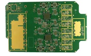
As a professional PCB supplier, Kingda focuses on providing reliable and high-quality circuit board solutions for different industries.
With experience in advanced PCB Manufacturing, Kingda supports:
- Multilayer PCB production
- Flexible PCB manufacturing
- High-density PCB solutions
- High-speed circuit board applications
- Customized PCB development
By combining engineering expertise, advanced production equipment, and strict quality control systems, Kingda helps customers achieve reliable PCB solutions from design verification to mass production.
Conclusion
A successful PCB Layout Design requires a comprehensive understanding of electrical performance, manufacturing technology, and application requirements.
Whether designing a traditional circuit board, a high-density Multilayer PCB, or a compact Flexible PCB, engineers must carefully consider:
- PCB Routing
- Signal Integrity
- Power distribution
- Electromagnetic Compatibility
- Manufacturing capability
Following professional PCB layout principles can significantly improve product reliability, performance, and production efficiency.
With continuous innovation in PCB technology, advanced design methods and manufacturing capabilities will continue to support the development of next-generation electronic products.