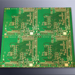
With the rapid development of electronic technology, electronic products are continuously evolving toward smaller sizes, higher integration, faster transmission speeds, and improved reliability. Behind almost every modern electronic device, from smart watches and smartphones to computers, communication equipment, automotive systems, and industrial control products, there is a core component that plays a critical role — the Printed Circuit Board (PCB).
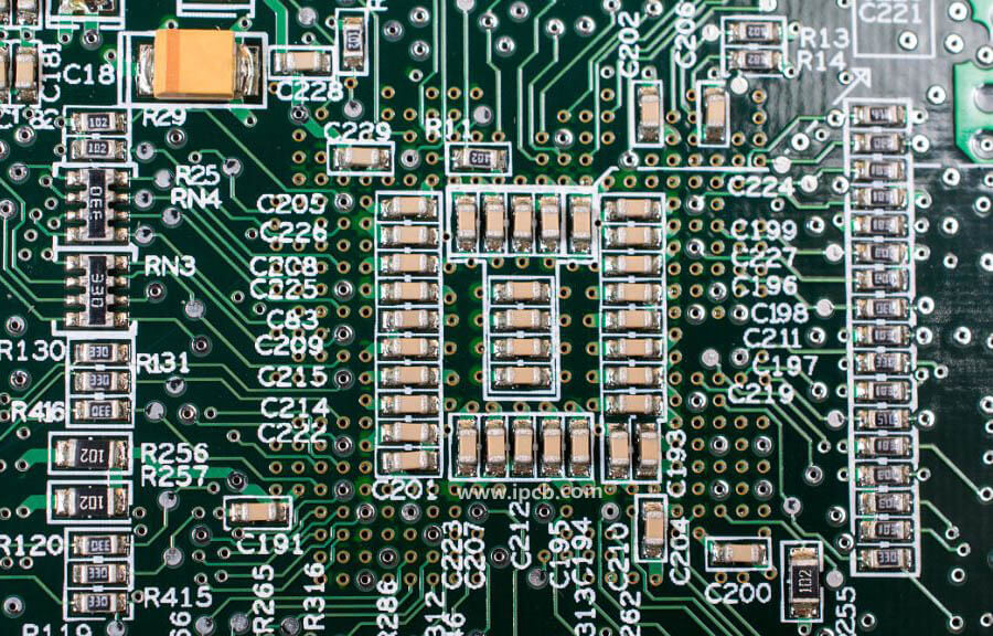
Printed Circuit Board is the abbreviation of PCB, which is one of the most important foundations of electronic manufacturing. A PCB is an insulating substrate with designed conductive patterns that provide electrical connections between electronic components. Through copper traces, pads, and vias, a PCB enables signal transmission and power distribution while providing mechanical support for electronic components.
In the early stages of electronic development, components were connected mainly through traditional wiring methods. However, as integrated circuits became smaller and electronic functions became more complex, traditional wiring could no longer meet modern requirements. The emergence of PCB Manufacturing technology solved these challenges by providing a standardized, reliable, and highly efficient method for electronic interconnection.
Today, almost all electronic products depend on advanced PCB Manufacturing processes. Without PCBs, integrated circuits, semiconductor devices, and electronic components would not be able to achieve stable electrical connections and reliable assembly.
As an experienced PCB supplier, Kingda focuses on providing high-quality PCB Manufacturing solutions, including prototype production, multilayer PCB fabrication, high-density PCB technology, and professional PCB assembly services.
What Is a Printed Circuit Board?
A Printed Circuit Board is a structure that uses insulating materials and conductive copper patterns to create electrical connections between electronic components.
The basic structure of a PCB usually includes:
- Copper layers
- Insulating dielectric materials
- Solder mask
- Silkscreen markings
- Component mounting pads
- Through holes and vias
The copper circuit pattern is manufactured according to the circuit design requirements. These conductive paths replace traditional wires and allow electrical signals to travel between components efficiently.
A PCB performs several essential functions:
1. Electrical Interconnection
The primary function of a Printed Circuit Board is to connect electronic components electrically.
Copper traces provide controlled paths for:
- Power transmission
- Signal transmission
- Ground connections
- High-speed data communication
For advanced electronic products, PCB design must consider signal integrity, impedance control, electromagnetic interference, and thermal management.
2. Mechanical Support
A PCB provides a stable physical platform for mounting electronic components.
Components such as:
- Integrated circuits
- Resistors
- Capacitors
- Connectors
- Sensors
are fixed onto the PCB surface through soldering technology.
This improves product durability and reduces wiring complexity.
3. Product Reliability Improvement
Modern PCB Manufacturing processes include strict quality control to ensure:
- Accurate circuit patterns
- Reliable solder joints
- Stable electrical performance
- Long product service life
High-quality PCB production is especially important for industries requiring high reliability, such as automotive electronics, medical equipment, aerospace systems, and communication infrastructure.
Types of Printed Circuit Boards
According to different structures, materials, and applications, Printed Circuit Boards can be divided into several major categories.
Flexible PCB
A Flexible PCB uses flexible insulating materials, usually polyimide or polyester film, as the substrate.
Unlike rigid boards, flexible circuits can bend, fold, and occupy limited spaces.
The main advantages of Flexible PCB include:
- Lightweight structure
- Excellent flexibility
- Space-saving design
- Resistance to vibration
- Suitable for compact electronic products
Flexible PCB technology is widely used in:
- Smartphones
- Wearable devices
- Cameras
- Medical equipment
- Automotive electronic systems
For products requiring three-dimensional assembly structures, flexible circuits provide significant design advantages.
Rigid PCB
A Rigid PCB is the most common type of circuit board used in electronic products.
Rigid boards typically use:
- FR-4 fiberglass materials
- Epoxy resin
- Copper foil layers
During production, copper foil is laminated onto the insulating substrate under high temperature and pressure to create a stable circuit structure.
Common rigid PCB structures include:
Single-Sided PCB
A single-sided PCB contains copper circuits on only one side of the substrate.
Features:
- Simple manufacturing process
- Low production cost
- Suitable for basic electronic products
Applications include:
- Simple controllers
- Household appliances
- Low-cost electronic devices
Double-Sided PCB
A double-sided PCB contains copper layers on both sides.
Through-hole plating technology connects the upper and lower copper layers, allowing more complex circuit designs.
Advantages include:
- Higher wiring density
- Better circuit performance
- More component placement options
Double-sided PCBs are widely used in:
- Industrial equipment
- Consumer electronics
- Control systems
Multilayer PCB
A Multilayer PCB consists of multiple copper layers stacked together with insulating materials.
Compared with single-sided and double-sided boards, multilayer PCBs provide:
- Higher circuit density
- Better signal performance
- Improved power distribution
- Reduced product size
Modern high-performance electronic products often use multilayer structures, including:
- 4-layer PCB
- 6-layer PCB
- 8-layer PCB
- 10-layer PCB
- High-layer-count PCB
Advanced applications may require more than 100 layers for extremely complex systems.
PCB Manufacturing Process Overview
The PCB Production Process is a highly complex manufacturing procedure involving multiple technologies, including:
- Material processing
- Photolithography
- Chemical treatment
- Electroplating
- Mechanical drilling
- Surface finishing
- Electrical testing
Unlike simple mechanical manufacturing, PCB production combines chemical, electrical, optical, and computer-controlled technologies.
Every production stage directly affects final PCB quality. A small defect during manufacturing may result in:
- Open circuits
- Short circuits
- Poor soldering
- Product failure
Therefore, strict process control is essential throughout the entire PCB Manufacturing process.
Single-Sided PCB Manufacturing Process
The basic manufacturing process of a single-sided Rigid PCB includes:
1. Material Preparation
Copper-clad laminate is selected according to PCB design requirements.
The material is cut into appropriate sizes before processing.
2. Drilling or Punching
Holes are created for component installation and mechanical positioning.
3. Circuit Pattern Formation
The circuit image is transferred onto the copper surface through printing technology.
The unwanted copper areas are removed through chemical etching.
4. Solder Mask Application
A solder mask layer is applied to protect copper circuits.
The solder mask provides:
- Oxidation protection
- Electrical insulation
- Prevention of solder bridging
Green is the most common solder mask color, but other colors such as black, blue, yellow, and red are also available.
5. Surface Treatment and Testing
The PCB receives surface finishing treatment before electrical testing.
Final inspection includes:
- Appearance inspection
- Electrical continuity testing
- Short circuit testing
After passing inspection, finished PCBs are packaged and delivered.
Double-Sided PCB Manufacturing Process
Compared with single-sided boards, Double-Sided PCB technology provides copper circuits on both sides of the substrate, allowing designers to create more complex electronic circuits.
The main manufacturing steps include:
1. Copper-Clad Laminate Preparation
The production begins with selecting suitable copper-clad laminate materials according to PCB design requirements.
Common materials include:
- FR-4
- High-frequency materials
- High-temperature resistant substrates
The material selection directly affects PCB electrical performance, mechanical strength, and reliability.
2. CNC Drilling Process
Precision CNC drilling equipment creates holes according to the PCB design data.
These holes include:
- Through holes
- Component holes
- Positioning holes
The drilling accuracy directly affects later plating and electrical connection quality.
3. Hole Cleaning and Deburring
After drilling, the PCB surface requires cleaning treatment.
This process removes:
- Drilling debris
- Resin residues
- Copper burrs
A clean hole wall ensures better copper plating quality.
4. Electroless Copper Plating
To achieve electrical connection between the two copper layers, the hole walls are coated with a thin copper layer.
This process is called through-hole metallization.
Afterward, additional copper plating increases the thickness and improves conductivity.
5. Circuit Pattern Transfer
The designed circuit image is transferred onto the copper surface through photolithography technology.
The process includes:
- Dry film lamination
- Exposure
- Development
- Circuit imaging
The exposed circuit areas are protected while unwanted copper is removed through etching.
6. Solder Mask and Surface Treatment
After circuit formation, a solder mask layer is applied.
The solder mask protects the PCB from:
- Oxidation
- Moisture
- Contamination
- Solder bridging
Then, according to application requirements, different surface finishes may be applied, including:
- HASL
- ENIG
- OSP
- Immersion Silver
- Immersion Tin
Multilayer PCB Manufacturing Process
The production of a Multilayer PCB is based on double-sided PCB technology but involves more complex manufacturing steps.
A multilayer PCB usually consists of:
- Inner copper layers
- Prepreg insulating materials
- Outer copper layers
- Solder mask layers
The main manufacturing process includes the following stages.
1. Inner Layer Circuit Manufacturing
The inner layers are produced first.
The process includes:
- Copper foil preparation
- Circuit imaging
- Etching
- Cleaning
- Inspection
After completing the inner circuits, automated optical inspection (AOI) is used to confirm circuit accuracy.
2. Layer Alignment and Lamination
Multiple inner layers are stacked together with insulating materials.
High temperature and pressure are applied during lamination to form a single integrated PCB structure.
This process requires extremely high alignment accuracy because even small deviations may affect electrical connections.
3. Mechanical Drilling and Laser Drilling
After lamination, holes are created according to design requirements.
Depending on PCB complexity, manufacturers may use:
- CNC mechanical drilling
- Laser drilling technology
Advanced PCB Manufacturing often uses laser drilling for microvias in HDI PCB applications.
4. Copper Plating
After drilling, the hole walls undergo chemical copper deposition.
This creates electrical connections between different layers.
The plating process requires precise control of:
- Copper thickness
- Uniformity
- Surface quality
5. Outer Layer Circuit Formation
The outer circuit pattern is created using:
- Dry film imaging
- Exposure
- Development
- Electroplating
- Etching
This forms the final conductive pattern of the multilayer PCB.
PCB Surface Protection and Finishing Process
During PCB Manufacturing, exposed copper surfaces must be protected because copper easily oxidizes when exposed to air.
Therefore, PCB manufacturers apply surface finishing treatments.
Common PCB Surface Finish technologies include:
HASL (Hot Air Solder Leveling)
Advantages:
- Low cost
- Good solderability
- Mature process
Suitable for standard PCB applications.
ENIG (Electroless Nickel Immersion Gold)
Advantages:
- Excellent flatness
- Long storage life
- Good corrosion resistance
Widely used for high-density and high-reliability products.
OSP (Organic Solderability Preservative)
Advantages:
- Environmentally friendly
- Smooth surface
- Suitable for fine-pitch components
Immersion Tin and Immersion Silver
These technologies provide:
- Good solderability
- Flat surface characteristics
- Compatibility with lead-free assembly
PCB Assembly and Surface Mount Technology
With the development of electronic products toward miniaturization, Surface Mount Technology (SMT) has become an essential part of modern PCB Assembly.
Traditional through-hole assembly requires component pins to pass through PCB holes. However, SMT directly mounts components onto PCB surfaces.
This technology provides:
- Higher component density
- Faster production speed
- Improved electrical performance
- Lower manufacturing cost
Main SMT PCB Assembly Process
1. Solder Paste Printing
The PCB enters the solder paste printing machine.
A stainless-steel stencil is placed above the PCB, and solder paste is accurately applied to component pads.
The printing quality directly affects solder joint reliability.
2. Component Placement
The Pick and Place Machine automatically places electronic components onto PCB pads.
Components include:
- Resistors
- Capacitors
- IC chips
- Connectors
- BGA devices
High-speed placement equipment ensures accuracy and efficiency.
3. Reflow Soldering
After component placement, the PCB enters the reflow oven.
The board passes through several temperature zones:
- Preheating
- Thermal soaking
- Reflow melting
- Cooling
The solder paste melts and forms permanent connections between components and PCB pads.
4. Inspection and Testing
Quality inspection is essential in modern PCB Assembly.
Common inspection methods include:
AOI Inspection
Detects:
- Missing components
- Wrong placement
- Solder defects
X-Ray Inspection
Used for hidden solder joints, such as:
- BGA
- QFN
- Advanced packages
Electrical Testing
Verifies:
- Circuit continuity
- Signal performance
- Product functionality
Development Trends of PCB Manufacturing Technology
As electronic products become smaller and more powerful, PCB Manufacturing technology continues to advance.
Future PCB development trends include:
1. High-Density Interconnect (HDI)
HDI technology improves wiring density through:
- Microvias
- Fine lines
- Smaller pads
It is widely used in:
- Smartphones
- 5G devices
- Advanced computing systems
2. Flexible and Rigid-Flex PCB
The combination of rigid and flexible structures allows designers to create compact and reliable electronic products.
Applications include:
- Wearable electronics
- Medical devices
- Automotive systems
3. High-Speed PCB Technology
Modern communication systems require PCBs with excellent signal performance.
Advanced designs focus on:
- Controlled impedance
- Signal integrity
- Power integrity
- Thermal management
4. Green PCB Manufacturing
Environmental protection has become an important direction in the PCB industry.
Manufacturers are increasingly adopting:
- Lead-free processes
- Environmentally friendly materials
- Waste reduction technologies
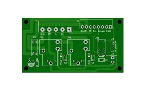
Kingda Professional PCB Manufacturing Capability
As an experienced PCB Manufacturing supplier, Kingda provides comprehensive PCB solutions for customers worldwide.
Kingda’s manufacturing capabilities include:
- Single-sided PCB production
- Double-sided PCB manufacturing
- Multilayer PCB fabrication
- Flexible PCB manufacturing
- High-density PCB solutions
- Professional PCB Assembly
Through advanced production equipment, strict quality control systems, and experienced engineering teams, Kingda helps customers develop reliable electronic products.
From prototype development to mass production, Kingda focuses on delivering stable quality, fast response, and customized PCB solutions.
Conclusion
The development of Printed Circuit Board technology has played a fundamental role in the evolution of modern electronics.
From simple single-sided boards to advanced Multilayer PCB, HDI, flexible circuits, and SMT assembly technologies, PCB manufacturing continues to move toward higher density, better performance, and greater reliability.
With the rapid growth of artificial intelligence, automotive electronics, communication systems, and smart devices, advanced PCB Manufacturing technology will continue to be a key foundation supporting future electronic innovation.