PCB Stencil for Precise SMT Solder Paste Printing
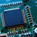
PCB assembly primarily uses two methods for mounting electronic components: Through-Hole Technology (THT) and Surface Mount Technology (SMT). THT connects components to a PCB by inserting component leads through drilled holes, while SMT places electronic components directly onto PCB pads using solder paste.
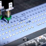
SMT has become the dominant assembly technology for modern electronic products and is often combined with THT in mixed-technology applications. During the SMT process, a PCB stencil is used to transfer a controlled amount of solder paste onto precisely defined PCB pads before component placement and reflow soldering. Proper stencil design and printing control are therefore essential for achieving reliable solder joints and consistent PCB assembly quality. GOPCBA provides comprehensive PCB assembly services for prototype, low-volume, and production requirements.
What Is a PCB Stencil?
A PCB stencil, also known as an SMT stencil or solder paste stencil, is a thin metal sheet used during the solder paste printing stage of SMT assembly. It contains precisely cut openings that correspond to the solder pads on a printed circuit board.
During printing, solder paste is spread across the surface of the stencil with a squeegee. The paste passes through the stencil apertures and is deposited onto the corresponding PCB pads. After the stencil is lifted away, the solder paste remains on the board in a controlled pattern ready for component placement.
A high-quality PCB stencil helps control:
- Solder paste volume
- Solder paste distribution
- Component placement accuracy
- Solder joint consistency
- Prevention of solder bridging
- Prevention of insufficient solder
- Overall SMT assembly reliability
Stencil printing is one of the most efficient methods for transferring solder paste accurately and repeatedly, making it especially important for automated and high-volume SMT production.
PCB Stencil Solder Paste Printing Process
PCB stencil printing is normally the first major step in the SMT assembly process. The quality of this stage directly affects component placement, reflow soldering, and final product reliability.
The following steps explain how a typical solder paste stencil printing process works.
1. Set Up the PCB Stencil
The PCB is positioned on the solder paste printer, and the stencil is securely mounted and clamped to prevent movement during printing.
Depending on production requirements, either manual or automated stencil printing equipment can be used. Automated systems are generally preferred for precision production because they provide more consistent alignment, pressure, and printing speed.
2. Apply Solder Paste
An appropriate amount of solder paste is placed onto the surface of the PCB stencil.
Before printing, the solder paste should be properly prepared according to the manufacturer’s storage and handling requirements. Solder paste viscosity, temperature, humidity, and working time can all affect printing performance.
The solder paste must remain consistent throughout the printing process to achieve stable transfer efficiency.
3. Align the PCB and Stencil
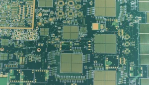
The PCB and stencil are precisely aligned so that each stencil aperture matches the corresponding solder pad on the PCB.
Accurate alignment is particularly important for fine-pitch components, BGA packages, QFN devices, and other high-density PCB designs.
Misalignment can cause solder paste to be deposited partially or completely outside the intended pad area, potentially resulting in solder bridges, insufficient solder, or component placement problems.
4. Move the Squeegee Across the Stencil
The squeegee moves across the stencil surface and pushes solder paste across the apertures.
As the squeegee passes over the stencil, solder paste is forced through the openings and deposited onto the PCB pads. Squeegee speed, pressure, angle, and paste condition all influence the quality and consistency of the print.
Proper process control helps achieve uniform solder paste deposits across the entire board.
5. Separate the Stencil from the PCB
After the solder paste has been deposited, the stencil is separated from the PCB.
Controlled stencil separation is especially important for fine-pitch applications. A stable separation process helps ensure that the solder paste remains on the PCB pads rather than being pulled away or smeared.
The finished PCB can then move to the component placement stage.
6. Inspect the Solder Paste
After printing, solder paste should be inspected to verify its position, volume, and consistency.
Automated inspection systems such as Solder Paste Inspection (SPI) can measure solder paste deposits and identify problems before components are placed.
Typical inspection parameters include:
- Solder paste volume
- Deposit height
- Deposit area
- Position accuracy
- Shape consistency
- Offset from the PCB pad
Early detection of printing defects helps prevent more serious problems during reflow soldering.
7. Clean the PCB Stencil
Stencil cleaning is an important part of maintaining consistent solder paste printing quality.
Solder paste residue can accumulate inside and around stencil apertures. If it is not removed regularly, the residue may harden or interfere with solder paste transfer during subsequent printing cycles.
Manual or automated stencil cleaning systems can be used depending on the production environment. For fine-pitch and high-density PCB assemblies, regular cleaning becomes even more important because small aperture openings are more sensitive to contamination.
Key Considerations in PCB Stencil Design
A properly designed stencil is essential for achieving reliable solder paste transfer. Several technical factors should be considered during PCB stencil design.
Stencil Geometry
PCB stencils are available in different sizes, shapes, and configurations. Aperture shapes are typically designed according to the corresponding PCB pad geometry and component requirements.
Important design parameters include:
- Stencil thickness
- Aperture size
- Aperture shape
- Pad dimensions
- Component pitch
- Solder paste characteristics
- Component package type
Stencil thickness directly affects the volume of solder paste deposited onto the PCB.
A thicker stencil generally deposits more solder paste, while a thinner stencil can be more suitable for fine-pitch components. If the stencil is too thick for a particular design, excessive solder paste may contribute to solder bridging.
For high-density PCB designs, aperture dimensions may need to be modified from the original PCB pad dimensions to achieve the desired solder paste volume and release performance.
Two important parameters commonly considered in stencil design are the area ratio and aspect ratio.
The area ratio compares the aperture opening area with the aperture wall area and is particularly important for determining solder paste release performance. The aspect ratio considers the relationship between aperture width and stencil thickness.
Both parameters should be evaluated when designing apertures for fine-pitch and miniature components.
PCB Stencil Materials
Stainless steel is the most widely used material for modern PCB stencils because of its strength, dimensional stability, corrosion resistance, and durability.
Stainless-steel stencils can maintain accurate aperture dimensions over repeated production cycles and are therefore suitable for both prototype and production SMT assembly.
Polymer-based stencil materials may also be used for specific applications. However, they generally do not provide the same durability and dimensional stability as stainless steel and are less common for demanding production environments.
Step Stencils
Step stencils, also called stepped stencils, are designed with different thickness levels within the same stencil.
This approach is useful when a PCB contains components with significantly different solder paste requirements. For example, fine-pitch components may require a thinner stencil area, while larger components may require a thicker region to achieve sufficient solder volume.
Step stencils can therefore help accommodate mixed component geometries on complex PCB assemblies without requiring separate stencils for different areas.
PCB Stencil Manufacturing Methods
PCB stencils are typically manufactured according to PCB layout data, commonly using Gerber files. Different manufacturing methods produce different aperture characteristics, edge qualities, and dimensional accuracy.
Laser Cutting
Laser cutting is one of the most widely used methods for manufacturing modern SMT stencils.
A precision laser creates individual apertures according to the stencil design data. Laser-cut stencils can provide accurate aperture dimensions and smooth, well-defined edges.
The process is particularly suitable for:
- Fine-pitch components
- BGA packages
- QFN packages
- High-density PCB layouts
- Small apertures
- Prototype and production applications
Laser-cut apertures can also be designed with suitable wall geometry to improve solder paste release.
Chemical Etching
Chemical etching is a subtractive manufacturing process in which unwanted metal is removed using chemical etchants.
The metal surface is first prepared and coated with a photoresist. The required pattern is then developed, and the exposed metal is chemically etched away.
Although chemical etching can be used for stencil manufacturing, its aperture characteristics may differ from those produced by precision laser cutting.
Electroforming
Electroforming is an additive manufacturing method that uses nickel to build the stencil structure.
The process can produce very smooth aperture walls and may be used when high solder paste release performance is required.
In some applications, electroforming may be combined with other stencil manufacturing technologies to achieve specific aperture requirements.
Common PCB Stencil Printing Problems and Solutions
Poor stencil design, incorrect printing parameters, or improper process control can cause several solder paste printing defects.
| Problem | Possible Cause | Recommended Solution |
|---|---|---|
| Printing Misalignment | PCB and stencil are not accurately aligned | Improve alignment accuracy and verify stencil registration before printing |
| Solder Bridging | Incorrect aperture geometry or excessive solder paste | Optimize aperture dimensions and control solder paste volume |
| Insufficient Solder | Apertures are too small or solder paste transfer is poor | Review aperture size, stencil thickness, and paste release performance |
| Solder Balls | Improper stencil design, excessive paste, or unsuitable printing conditions | Optimize stencil thickness, aperture geometry, and printing parameters |
| Uneven Solder Deposits | Inconsistent squeegee pressure, speed, or solder paste condition | Maintain stable printing parameters and solder paste conditions |
| Paste Smearing | Poor stencil separation or excessive paste residue | Optimize separation settings and clean the stencil regularly |
How to Choose the Right PCB Stencil
Selecting the correct stencil depends on the PCB design, component package, solder paste, and assembly process.
Key factors to evaluate include:
- PCB pad geometry
- Smallest component pitch
- BGA and QFN requirements
- Required solder paste volume
- Stencil thickness
- Aperture shape and size
- Assembly technology
- Prototype or production volume
- Leaded or lead-free solder paste
- Required printing accuracy
For complex PCBs, stencil design should ideally be reviewed together with the PCB layout and assembly process. This helps identify potential solder paste printing issues before production begins.
 GOPCBA PCB Stencil and SMT Assembly Support
A reliable PCB stencil is an important part of a stable SMT manufacturing process. Proper stencil design, accurate manufacturing, controlled solder paste printing, and effective inspection all contribute to consistent PCB assembly quality.
GOPCBA supports customers with integrated PCB manufacturing and assembly solutions, including SMT assembly, through-hole assembly, mixed-technology assembly, PCB fabrication, component sourcing, testing, and related manufacturing services.
For projects requiring stencil-based solder paste printing and complete PCB assembly, you can submit your PCB design files, Gerber files, BOM, and other relevant production information for engineering evaluation. Our team can help determine suitable stencil specifications and assembly processes for your application.
For project consultation and production requirements, please contact GOPCBA to discuss your PCB stencil and SMT assembly needs.