



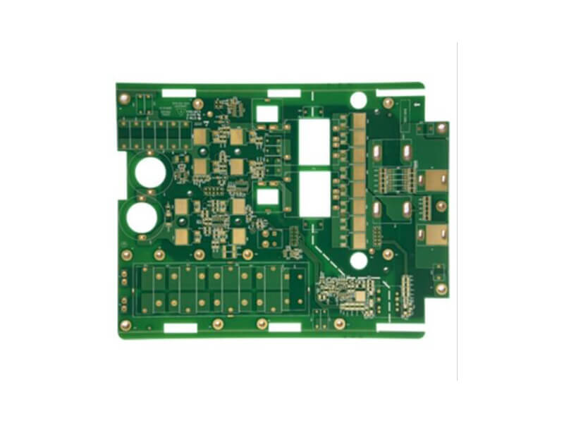
PCB Outline Design: Outline Layer, Panelization and Tolerances
Most layout reviews spend their time on impedance and length matching and treat the board edge as a formality. The edge is what the fabricator machines first, what the assembler clamps, and what decides whether a thin product survives its own reflow profile. Getting the PCB outline design right costs an hour in the CAD tool and saves a tooling revision.
The Outline Layer and Its Names
Every CAD package has a layer that defines where the board will be cut. Depending on the tool it is called the board outline layer, the mechanical layer, or the outline layer, and the names hide an important fact: only one of them should be authoritative. If the fabricator receives two overlapping closed contours, or one contour on the mechanical layer and another on the keepout layer, the CAM engineer has to guess. Guessing produces boards cut along the wrong contour, and there is no way to recover a panel once it has been routed.
The practical rule is to draw one closed contour of zero-width lines on a dedicated layer, place it in the centre of the board, and state in the fabrication drawing which layer that is. Delete or clearly mark any historical contours left over from an earlier revision.
Keepout Versus Mechanical Layer
Keepout layers express where components and copper may not go. They do not define the cut. Mixing them means the copper pullback distance is decided by whoever reads the file last, and the difference between a 0.3 mm and a 0.5 mm pullback is enough to change the impedance of an edge-coupled line. Keep the copper-to-edge clearance explicit, 0.3 mm being a common default for routed edges, and state it rather than inheriting it.
Minimum and Maximum Outline Dimensions
Fabricators publish a workable range, typically from 5 mm square up to the panel size, but the useful range is narrower. Boards smaller than about 30 mm on a side are awkward to handle, and both the routing and the surface finish steps become less uniform, so they are normally delivered in a panel. Above roughly 500 mm, thickness and flatness have to be checked against the conveyor and the placement machine, and the fabricator will want to know about stiffeners or a heavier core before quoting.

Overhanging features deserve their own limit. A narrow tab that sticks out of the main outline is easy to break in handling, so keep such features at least 2 mm wide and under 10 mm long to avoid the cracked base material that appears later as a cosmetic reject or, worse, as a mechanical failure in the field.
Milling, Routing Tolerance and Edge Quality
The edge is produced by a router bit, and the routing tolerance the bit can hold is typically plus or minus 0.15 mm on a standard process, tightening to 0.1 mm on a controlled one. That number has to be reconciled with the mechanical design, because a connector designed to sit flush with the edge will show a visible step on one side of the panel and sit proud on the other. Where edge position matters functionally, design a pocket or a reference feature instead of relying on the outline.
Panelization and Breakaway Design
panelization decides how the board is presented to the assembly line, and it is the step where outline decisions get expensive. The array has to fit the stencil and the conveyor, leave room for fiducials and tooling holes, and still break cleanly after reflow. Two methods dominate. A V-cut scores both sides of the panel and gives a clean straight break with no material left behind, but it only works on straight lines and needs a minimum remaining thickness so the panel does not fall apart on the line. Stamp holes, a row of small perforations, handle curved and irregular shapes and leave a small tab that must be trimmed or designed into a recess.

Whichever method is used, keep the breakaway line at least 1 mm clear of components and place the rails so the machine can clamp the panel without touching a part. Router-cut arrays with removable rails are the most flexible option and the most expensive, which is why the outline should be settled before the panel is laid out rather than after.
Thin Boards and Thickness Control
Products below 1 mm final thickness change the rules. The laminate is flexible, so a 0.6 mm board in a panel will bend under its own weight and the handling tolerance has to be negotiated in advance. Thickness tolerance is often plus or minus 10 percent on thin cores and the flatness specification has to be agreed explicitly. Backing sheets and a stiffer panel help, and so does a simple outline, since every sharp internal corner concentrates the stress that leads to warping.
Flatness, Bending and Component Stress
Fewer bends and fewer corners along the outline mean less stored stress. A board with a long narrow neck flexes more easily than a rectangular one, and flexing transfers directly into the solder joints of the largest components. If the outline has to be irregular, keep the neck wide, keep fine-pitch parts off the narrow section, and consider a stiffener. PCB dimensional stability is measurable, so ask for the flatness figure rather than assuming it.
Connectors, Mounting and Service Access
Outline design and mechanical design meet at the interfaces. Connectors need edge clearance for the mating shell, mounting holes need a keepout for the screw head and washer, and anything that will be serviced needs a route for a probe or a tool. Board outline and mounting design is best reviewed with the enclosure in hand: if the boss and the hole disagree by 0.2 mm, no tolerance on the PCB will save the assembly.
Give the connectors a defined datum as well. When the outline is the datum for everything else, the routing tolerance propagates into the connector position, and a 0.15 mm error becomes a 0.15 mm misalignment in the finished product.
Slot and Edge Features
Internal slots follow their own rules. A slot narrower than the router bit cannot be cut, and an inside corner always carries the bit radius, so a sharp internal corner is really an arc of 1 mm or more. Design the corner radius explicitly instead of discovering it on the first article. PCB slot design rules and edge routing cover minimum slot width and the clearance between a slot and nearby copper, both of which are much easier to plan than to fix.
FAQ
Which layer should carry the board outline? One dedicated layer, with a single closed zero-width contour, named in the fabrication drawing. Do not duplicate the contour onto the keepout layer, and remove contours from earlier revisions so the CAM engineer has exactly one interpretation.
When is V-cut better than stamp holes? Use V-cut for straight break lines on rectangular arrays where the panel can keep enough material to stay rigid. Use stamp holes for curved outlines, mixed shapes and boards that must break without leaving a burr on a visible edge.
How tight should an outline dimension be? Specify what the function needs. A cosmetic edge can live with plus or minus 0.2 mm, a connector datum usually cannot. Tightening the whole outline to 0.1 mm costs money, so apply it only where a mating part is involved.


