Before committing to a full production run of printed circuit boards, engineers need to confirm that the design works as intended. PCB prototyping provides an efficient way to build a small number of boards, test electrical and mechanical performance, identify design problems, and optimize the product before mass production.
A well-executed PCB prototype does more than prove that a circuit works. It can reveal issues related to signal integrity, thermal management, component availability, manufacturability, assembly, and product integration.
For startups, R&D teams, electronics engineers, and OEMs, an efficient prototype PCB assembly process can reduce development risk, shorten the product development cycle, and make the transition from prototype to volume production much smoother.
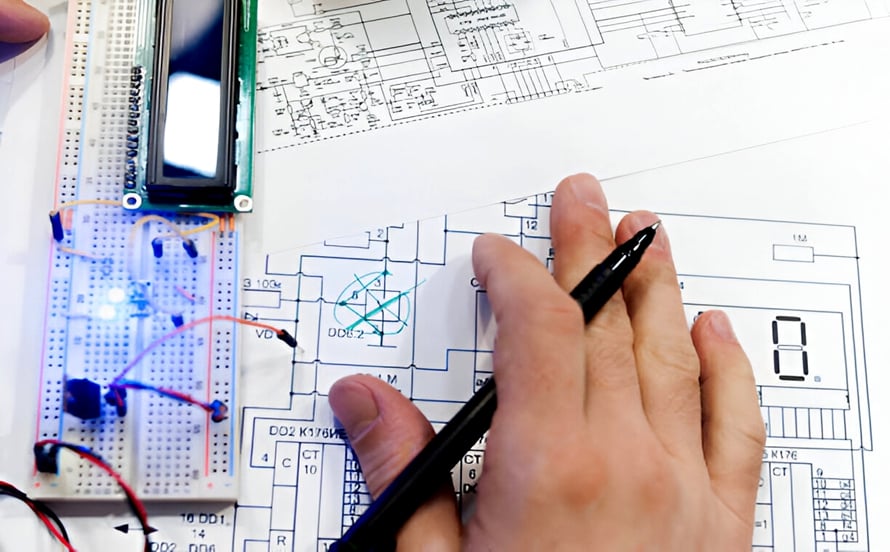
This guide explains the complete PCB prototyping process, from design preparation and PCB fabrication to component sourcing, SMT assembly, inspection, functional testing, and production transfer.
What Is PCB Prototyping?
A PCB prototype is an initial physical version of a printed circuit board manufactured in a relatively small quantity for engineering evaluation and product validation.
Unlike volume production, where the primary objectives are consistency, throughput, and cost optimization, PCB prototype manufacturing focuses on:
- Design verification
- Functional testing
- Manufacturing validation
- Component validation
- Thermal evaluation
- Signal integrity testing
- Mechanical fit testing
- Firmware and software development
The prototype bridges the gap between a digital PCB design and a production-ready electronic product.
PCB Fabrication vs. PCB Prototype Assembly
It is important to distinguish between PCB fabrication and PCB assembly.
PCB fabrication converts the digital PCB layout into a physical bare board. This includes the substrate, copper layers, vias, solder mask, silkscreen, surface finish, and board outline.
PCB prototype assembly then mounts electronic components onto the fabricated board using SMT, THT, or mixed assembly processes.
A complete prototype development cycle therefore looks like:
PCB Design → PCB Fabrication → Component Sourcing → PCB Assembly → Inspection → Functional Testing → Design Optimization
The combination of fabrication and assembly enables engineers to evaluate the complete electronic system rather than testing only the bare circuit board.
Why Is PCB Prototyping Important?
Creating a prototype before mass production can provide several important engineering and commercial benefits.
Early Detection of Design Problems
A prototype can reveal problems that are difficult to identify through schematic review or simulation alone.
Typical examples include:
- Incorrect component footprints
- Signal-integrity problems
- Crosstalk
- Power distribution problems
- Excessive heat
- Incorrect component orientation
- Mechanical interference
- Insufficient PCB clearance
- Assembly difficulties
Finding these issues before mass production can prevent expensive tooling, inventory, rework, and production delays.
Faster Design Validation
A functional prototype provides real-world evidence of whether the design meets its intended electrical and mechanical requirements.
Engineers can evaluate:
- Voltage and current
- Signal quality
- Communication interfaces
- Power consumption
- Thermal behavior
- Sensor performance
- Firmware operation
- Mechanical fit
The resulting data can then be used to refine the next PCB revision.
Reduced Product Development Risk
A production mistake can affect thousands of boards. A prototype allows the engineering team to identify and correct problems while production quantities are still small.
This makes prototype PCB assembly an important risk-reduction stage between engineering design and mass production.
Faster Time to Market
A fast prototype cycle allows engineers to complete multiple design iterations without waiting several weeks between revisions.
This is particularly valuable for:
- IoT products
- Consumer electronics
- Automotive electronics
- Medical electronics
- Industrial automation
- AI hardware
- Communication equipment
Better Preparation for Mass Production
Prototype production should not be treated only as a functional test. It should also provide information about how the product will behave during manufacturing.
A good prototype process can identify:
- Assembly constraints
- Component sourcing problems
- DFM issues
- DFT requirements
- Test-point requirements
- Stencil limitations
- Reflow issues
- Panelization opportunities
These findings make the transition to volume PCB assembly more predictable.
Before Starting PCB Prototyping
Not every design requires the same prototype strategy.
For an existing product with a proven PCB design, a new prototype may not be necessary for every production cycle. However, prototypes are strongly recommended when:
- Introducing a new PCB design
- Changing major components
- Changing PCB materials
- Adding high-speed interfaces
- Modifying the PCB stackup
- Changing mechanical dimensions
- Introducing new manufacturing processes
- Moving to a new assembly partner
The prototype quantity should also reflect the engineering objective.
For example:
1–5 boards: Basic design verification
5–20 boards: Engineering validation and debugging
20–100 boards: Pilot testing and system validation
100+ boards: Pre-production and manufacturing validation
The exact quantity should be determined by product complexity, testing requirements, and project objectives.
PCB Prototype Design Preparation
Before requesting a prototype quote, engineers should prepare a complete manufacturing package.
PCB Layer Count
Specify:
- Number of layers
- Signal layers
- Power layers
- Ground planes
- HDI structures if applicable
Simple products may require only two layers, while high-density or high-speed applications may require multilayer or HDI construction.
Board Thickness
Specify the required PCB thickness and applicable tolerance.
Typical applications may use standard board thicknesses, but mechanical or high-current applications may require special thicknesses.
Copper Thickness
Copper weight directly affects:
- Current-carrying capability
- Thermal performance
- Trace resistance
- Manufacturing cost
High-current applications may require heavy copper or additional copper reinforcement.
Trace Width and Spacing
The minimum trace width and spacing should be compatible with the selected manufacturer’s capabilities.
For advanced boards, engineers should confirm:
- Minimum line width
- Minimum spacing
- Controlled impedance
- Differential-pair requirements
- RF routing requirements
Hole and Via Requirements
Provide:
- Minimum drill diameter
- Finished hole size
- Via type
- Annular ring requirements
- Blind vias
- Buried vias
- Microvias
- Via-in-pad structures
Complex via structures can significantly affect prototype cost and lead time.
Surface Finish
Common options include:
- HASL
- Lead-free HASL
- ENIG
- ENEPIG
- OSP
- Immersion tin
- Immersion silver
The correct finish depends on assembly technology, environmental conditions, shelf life, and component package requirements.
Solder Mask and Silkscreen
Specify:
- Solder-mask color
- Silkscreen color
- Solder-mask clearance
- Silkscreen text
- Polarity markings
- Component reference designators
Essential PCB Prototype Manufacturing Files
A professional prototype PCB assembly project should provide a complete and consistent documentation package.
Gerber or ODB++ Files
Manufacturing files should include:
- Copper layers
- Solder mask
- Silkscreen
- Board outline
- Drill files
- Additional fabrication data
ODB++ and IPC-2581 can also provide richer manufacturing information than conventional Gerber-only workflows.
Bill of Materials
The BOM should include:
- Reference designator
- Manufacturer
- Manufacturer Part Number (MPN)
- Component description
- Package
- Quantity
- Approved alternatives
- DNP information
Avoid vague descriptions such as:
10 µF capacitor
A better BOM identifies the exact electrical, mechanical, and manufacturer-specific requirements.
Pick-and-Place File
The Centroid file should provide:
- Reference designator
- X coordinate
- Y coordinate
- Rotation
- PCB side
The coordinate origin must be consistent with the PCB manufacturing data.
Assembly Drawing
The assembly drawing should indicate:
- Component orientation
- Polarity
- Pin 1
- DNP components
- Special assembly instructions
- Mechanical restrictions
Stackup and Impedance Information
For high-speed PCB designs, provide the stackup and impedance requirements before manufacturing.
This is particularly important for:
- USB
- PCIe
- Ethernet
- DDR
- HDMI
- RF
- 5G
- High-speed SerDes
PCB Prototyping Process
Once the design package has been reviewed, the prototype moves into manufacturing.
1. PCB Design Review
The manufacturer’s engineering team examines the design for potential manufacturing issues.
A DFM review may identify:
- Trace-width problems
- Clearance violations
- Drill limitations
- Solder-mask issues
- Incorrect footprints
- Via problems
- Board-edge issues
A DFA review can identify potential assembly problems before the board reaches production.
Kingda provides engineering review and DFM/DFMA support as part of its PCB and PCBA services. (Kingda)
2. PCB Fabrication
The bare PCB is then manufactured.
Typical steps include:
Material Preparation → Inner-Layer Imaging → Etching → Lamination → Drilling → Copper Plating → Outer-Layer Imaging → Solder Mask → Surface Finish → Silkscreen → Electrical Testing
For advanced PCB structures, the process may additionally involve:
- Laser drilling
- Sequential lamination
- Microvia formation
- Copper-filled vias
- Impedance-controlled fabrication
Kingda’s published PCB capabilities include multilayer, HDI and advanced PCB structures, with standard and advanced capability ranges extending to high layer counts, fine trace/space dimensions, laser drilling, stacked microvias and copper-filled microvias. (Kingda)
3. Component Sourcing
Once the bare boards are completed, components are sourced according to the BOM.
A professional supplier should verify:
- Component availability
- Lead time
- Lifecycle status
- Approved alternatives
- Supplier authenticity
- Date-code requirements
- MSL requirements
Kingda provides component procurement and maintains supply-chain relationships with major distributors, supporting turnkey, partial-turnkey and customer-supplied component models. (Kingda)
4. Solder Paste Printing
For SMT assembly, solder paste is applied through a precision stencil.
Printing quality depends on:
- Stencil thickness
- Aperture geometry
- Solder paste properties
- Squeegee pressure
- Printing speed
- Board support
- Stencil alignment
SPI (Solder Paste Inspection) can then verify the solder-paste deposition before component placement.
5. Pick-and-Place Assembly
Automated placement machines position the components according to the Centroid file.
The machine verifies:
- Component identity
- Position
- Rotation
- Polarity
- Placement accuracy
Modern SMT systems can handle very small packages and fine-pitch components.
Kingda’s published prototype capabilities include 01005 and 0201 components, 0.25 mm-pitch BGA, QFN and high-precision IC placement. (Kingda)
6. Reflow Soldering
The assembled board passes through a controlled reflow oven.
The temperature profile must match the solder paste and component requirements.
A correct reflow process helps prevent:
- Cold solder joints
- Solder bridging
- Tombstoning
- Insufficient wetting
- Component damage
- Excessive thermal stress
7. Through-Hole Assembly
Some prototypes also require THT components.
Through-hole components may be installed through:
- Manual insertion
- Automated insertion
- Wave soldering
- Selective soldering
Kingda supports manual and automated through-hole assembly, wave soldering, selective soldering, lead-free processes, conformal coating, IC programming, inspection and functional testing. (Kingda)
8. Inspection and Quality Control
Quality control is critical even for a prototype.
Common inspection methods include:
Visual Inspection
Used to identify obvious defects such as:
- Missing components
- Wrong orientation
- Damaged components
- Soldering problems
AOI
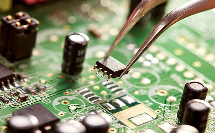
Automated Optical Inspection checks component placement and visible solder joints.
X-Ray Inspection
X-ray inspection is particularly useful for:
- BGA
- QFN
- LGA
- Hidden solder joints
Kingda’s rapid prototype service states that prototypes receive 100% X-ray and AOI testing, with ICT, FCT and FAI testing also available. (Kingda)
9. Functional Testing
Functional testing verifies that the completed prototype performs according to its intended application.
Depending on the product, testing may include:
- Power-up tests
- Communication testing
- Sensor verification
- Firmware programming
- Display testing
- Motor control
- RF testing
- Analog measurement
- Digital interface testing
Functional testing should ideally use the same test strategy that will eventually be applied to production units.
Factors Affecting PCB Prototype Cost and Lead Time
Several factors determine prototype cost.
Board Complexity
A simple two-layer board is generally easier and faster to produce than a complex multilayer HDI design.
Factors include:
- Layer count
- Board size
- Trace width
- Via structure
- Surface finish
- Copper thickness
- Special materials
Component Count
A PCB with 30 components is generally easier to assemble than one with several hundred components.
Component density also affects:
- Placement time
- Stencil complexity
- Inspection requirements
- Rework difficulty
Component Availability
Component procurement can become one of the largest prototype schedule constraints.
A board may be fabricated quickly, but one unavailable IC can delay the entire assembly.
Testing Requirements
Basic AOI is different from a complete functional test.
Additional requirements such as:
- X-ray
- ICT
- FCT
- Environmental testing
- Burn-in
- Reliability testing
can increase both cost and lead time.
Quantity
Small quantities usually have higher unit costs because setup, programming, engineering and tooling costs are distributed across fewer units.
However, panelization can improve efficiency.
How to Reduce PCB Prototype Cost
Use Standard Materials
When the design does not require specialized materials, standard FR-4 can help reduce cost and lead time.
Use Readily Available Components
Selecting widely available components can reduce sourcing risk.
Minimize Unnecessary Complexity
Do not use HDI, microvias or exotic materials unless the application actually requires them.
Panelize Small Boards
Panelization allows multiple prototypes to be assembled efficiently in one production run.
Complete DFM Before Manufacturing
Finding a problem before production is much less expensive than correcting it after fabrication.
Use Pre-Approved Alternatives
For generic passives and standard components, approved substitutes can prevent unnecessary procurement delays.
Testing the Prototype After Assembly
Prototype assembly is not the end of the engineering process.
The completed prototype should be evaluated under realistic operating conditions.
Electrical Testing
Test:
- Voltage
- Current
- Resistance
- Communication
- Signal integrity
- Power consumption
Thermal Testing
Measure:
- Component temperature
- PCB temperature
- Heat concentration
- Thermal cycling behavior
Mechanical Testing
Where relevant, evaluate:
- Vibration
- Shock
- Connector durability
- Board fit
- Enclosure integration
Firmware Testing
For embedded systems, verify:
- Boot sequence
- Communication interfaces
- Sensors
- Control functions
- Error handling
- Firmware compatibility
If the prototype fails, the design should be revised and another prototype iteration produced.
This design-build-test-revise cycle is one of the most important aspects of modern electronics development.
Prototype-to-Production Transition
One of the biggest advantages of using an experienced PCB assembly manufacturer is the ability to transition from prototypes to volume production without completely restarting the manufacturing process.
The prototype should therefore be designed with future production in mind.
Important considerations include:
- Component availability
- PCB panelization
- SMT placement efficiency
- Test-point accessibility
- DFM
- DFA
- Manufacturing yield
- Component lifecycle
- Supply-chain stability
Kingda supports the complete path from rapid PCBA prototyping and low-volume production to volume manufacturing, allowing the same manufacturing partner to support different stages of the product lifecycle. (Kingda)
Why Choose Kingda for PCB Prototype Assembly?
Kingda is a China-based one-stop PCB and PCBA manufacturer providing PCB fabrication, component procurement, SMT, through-hole assembly, testing and final product integration. (Kingda)
Rapid Prototype Capability
Kingda’s published prototype service includes:
- No minimum order quantity
- SMT assembly
- Through-hole assembly
- Mixed assembly
- Fine-pitch components
- 01005 and 0201 components
- BGA and QFN
- X-ray and AOI inspection
- ICT and FCT
- IC programming
- FAI testing
Its published prototype lead time is normally 2–3 days, with an expedited option as fast as 12 hours, depending on project conditions and component availability. (Kingda)
Advanced Manufacturing Equipment
Kingda states that its PCBA production uses 8 fully automated production lines, supporting rapid SMT assembly and high-precision component placement. (Kingda)
Wide PCB Technology Coverage
Kingda supports:
- Rigid PCB
- Flexible PCB
- Rigid-flex PCB
- Multilayer PCB
- HDI PCB
- High-frequency PCB
- High-speed PCB
- Heavy-copper PCB
- Advanced interconnect structures
Its published PCB capabilities include stacked and copper-filled microvias for HDI applications. (Kingda)
One-Stop Manufacturing
Instead of coordinating separate PCB fabrication, component sourcing and assembly suppliers, customers can use one integrated workflow covering:
PCB Design → DFM → PCB Fabrication → Component Procurement → SMT/THT → Testing → Final Assembly
This helps simplify supplier communication and supports faster prototype-to-production transitions. (Kingda)
PCB Prototype Assembly Checklist
Before submitting a prototype order, confirm that you have:
Design Files
- Gerber or ODB++ files
- Drill files
- PCB outline
- Stackup
- Impedance requirements
Assembly Files
- Complete BOM
- MPNs
- Pick-and-place file
- Assembly drawing
- DNP information
- Polarity information
Manufacturing Requirements
- PCB material
- Layer count
- Board thickness
- Copper thickness
- Surface finish
- Solder-mask color
- Silkscreen requirements
Testing Requirements
- AOI
- X-ray
- ICT
- FCT
- Firmware programming
- Special reliability tests
A complete data package allows the manufacturer to perform a more accurate quotation and engineering review.
Conclusion
PCB prototyping is one of the most important stages between electronic design and mass production. It gives engineers the opportunity to transform a digital design into a physical product, verify performance, identify manufacturing problems, and optimize the design before committing to large production quantities.
The most effective prototype strategy is not simply to make a small number of boards as quickly as possible. It is to create prototypes that accurately reflect the eventual manufacturing process.
A professional prototype PCB assembly service should therefore provide:
PCB Fabrication + Component Sourcing + SMT/THT Assembly + DFM + AOI + X-Ray + Functional Testing + Engineering Support
Kingda’s integrated PCB and PCBA capabilities support this full development path, from rapid prototype assembly and low-volume manufacturing through volume production. Its published prototype capabilities include no MOQ, rapid turnaround, advanced SMT assembly, 01005 components, fine-pitch BGA, X-ray/AOI inspection and functional testing. (Kingda)
For engineers developing a new electronic product, building a well-controlled prototype before mass production can significantly reduce manufacturing risk and create a much smoother transition from PCB design to production-ready electronics.