The Role of the PCB in the Electronics Production Process
A consumer electronic product is usually judged by its case, but the schedule is normally set by the board inside it. In the electronics production process the printed circuit board is the item that connects the industrial design, the firmware and the factory.
How a Product Programme Starts
A programme begins with an idea about how the product should look and what it should do. Sketches and rendered models are produced first, and the shape is discussed long before anyone knows how much board area will be available inside it.
The first engineering question is whether the concept can be built at a price the market will accept. That question is answered by the enclosure volume, the connector positions and the number of functions the board has to support.
Enclosure Design and the Mechanical Envelope
Enclosure design fixes the internal envelope that the board must fit. Ribs, bosses, battery compartments and the lens or display aperture all take space, and the remaining volume has to accommodate the board, its components and the clearance around them.
The mechanical team produces a first article of the case, often a machined or cast prototype. It is checked against the board outline and the connector cut outs, and any interference found here is corrected before tooling is committed.
Schematic and Netlist
Once the function list is agreed, the hardware engineer draws the schematic and converts it into a netlist. The netlist is what the layout tool consumes, and it is also the reference for the bill of materials that purchasing will use.
Component choice happens at the same time. Parts that are single sourced, near end of life or only available in a package that the factory cannot place are better replaced before the layout begins than after the panels arrive.
Defining the PCB Outline
The pcb outline comes from the mechanical model, and the mounting holes, the connector openings and the keep out zones are copied from it directly. Approximating these features by eye is a common source of a first build that will not assemble.
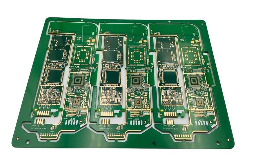
The outline is also a manufacturing decision. Panel rails, break away tabs and the minimum distance from the edge to copper all depend on it, and they are easier to accommodate when the shape is simple and the corners are not unnecessarily tight.
Placement Under Mechanical Constraints
Placement is a negotiation between the circuit and the case. Components with a height limit have to be kept clear of the lid, the user interface has to align with the openings, and the connector bodies must match the wall thickness of the housing.
Thermal and mechanical needs pull in the same direction. The parts that dissipate power want copper and clearance, and the parts that are heavy want to sit near a mounting point rather than at the centre of an unsupported span.
Power and Ground Routing
Power and ground are routed before the signal nets, because they define the planes and the current paths that everything else depends on. A converter that has a short, wide loop behaves very differently from one that has been routed around the board.
On a thin handheld product the ground plane is also the return path for the radio and the display, so it is worth checking that the plane is continuous under the sensitive circuits before the signal routing is finalised and hard to change.
The Prototype Build
The first prototype build brings together the board, the case, the battery and the display. It is assembled by hand, soldered, programmed and tested, and it is the first point at which the three disciplines meet on real hardware.
Prototype boards should be produced with the same stackup and finish as the intended production part wherever the budget allows. A prototype that is built differently can pass the bench test and still fail when the real process is used.
Debugging the First Boards
Debug normally starts with the power rails and the clock, because almost everything else depends on them. From there the engineer checks the boot sequence, the memory interface and the communication with each peripheral in turn.
Faults found at this stage are usually corrected with a wire link or a component change on a small number of boards. That is an acceptable way to keep a programme moving, as long as the layout is corrected in the next revision.
Design Iteration
Each design iteration should have a defined objective rather than a list of wishes. Grouping the fixes into a revision that can be verified in one build keeps the cost of tooling and the number of engineering builds under control.
The number of iterations a product needs is often decided by how well the mechanical and electrical sides communicate. A board that is designed against a frozen mechanical model needs fewer revisions than one designed against a description.
Tooling and the Schedule
Injection moulds take weeks to cut and cannot easily be changed afterwards, so the case is usually frozen before the board is final. That is why the board dimensions and the connector positions matter so much during the early phase.
From the moment tooling is released, the schedule is driven by the longest lead item. Printed circuit boards are fast by comparison, which is why late electrical changes are absorbed by board revisions rather than by changes to the housing.
Design for Manufacture and Assembly
A design that works on the bench still has to pass through the assembly line. Placement orientation, panel utilisation, fiducials and the reflow profile all affect the yield, and they are decided by the layout rather than by the process engineer.
Assembly notes belong with the fabrication data. The written requirement travels with the board, so the process used in production matches the one that was validated during the prototype build.
Test Points and Production Test
Production test needs access to the nodes that prove the board is working. Programming pads, a serial header and a few measurement points turn a functional test from a manual operation into a fixture that runs in seconds.
The fixture is designed around the layout, so test access is much cheaper when it is planned at design time. Adding pads to a released board costs a revision; adding them during layout costs nothing.
Documentation and Handover
At handover the factory needs the Gerber data, the drill file, the stackup, the bill of materials and the assembly drawing, all from the same revision. It also needs the fabrication notes that describe anything outside the standard process.
A short release checklist keeps those items together. The practical details are in our design and fabrication and PCBA development notes, which follow a build from the first schematic to the tested assembly.
Why the Board Sets the Pace
The board is the only item in a product that touches every other discipline. It carries the firmware, it fits the case, it is placed by the assembly line and it is tested by the fixture, so its revision date often becomes the programme date.
Planning the layout sequence early, with the mechanical model frozen and the components selected, is the practical way to keep that date realistic. Component placement and pad definition follow the same thinking, and our note on placement order and pad positioning covers it in more detail.
FAQ
Should the case or the board be designed first? The enclosure concept comes first because it sets the available volume, but the board outline is fixed as soon as a mechanical model exists. Working from a frozen model is what avoids a late redesign.
How many prototype rounds are normal? Two or three builds are typical for a new product. The number falls when the mechanical and electrical data are frozen together and rises when each side keeps changing independently.
Why do prototype boards sometimes behave differently from production? Because the stackup, the finish or the assembly process was changed for the prototype. Keeping those parameters identical is the simplest way to make the test meaningful.