Four Layer PCB Design Process From Schematic to Gerber
A four layer board is the first stackup that gives a designer dedicated power and ground planes, and that changes the way the job is planned. The four layer pcb design process is not a longer version of a two layer layout; it is a different order of decisions.
What the Extra Layers Buy
The two inner layers normally carry ground and power, which leaves both outer layers free for signals. Every trace then has a reference plane close to it, so the return current flows directly underneath the signal instead of finding an indirect path.
That benefit only materialises when the planes stay continuous. A plane split by a slot forces the return current to detour around the obstacle, which increases loop area, adds inductance and radiates. Treat plane integrity as a routing constraint from the first day of layout.
Schematic Capture
Schematic capture fixes the connectivity of the whole design. Draw symbols and footprints at the same time, because a symbol with no matching footprint is normally discovered only after the data has been transferred to the layout tool.
Run the electrical rule check before anything is exported. Unconnected pins, conflicting outputs and undriven nets are far cheaper to resolve on the schematic sheet than in copper, and hierarchical sheets keep a large design readable for the engineer who inherits it.
Planning the Board Before Layout
Settle the outline, the mounting holes, the connector positions and the layer count before placing a single part. Mechanical interfaces are the least negotiable items in the project, and moving them after routing has started discards work that cannot be recovered.
Decide at the same time whether parts go on one side or both. Two sided assembly halves the required area but doubles the process steps and the tooling, and it changes which nets have to reach across the board instead of staying local.
Setting Up Rules and Layer Parameters
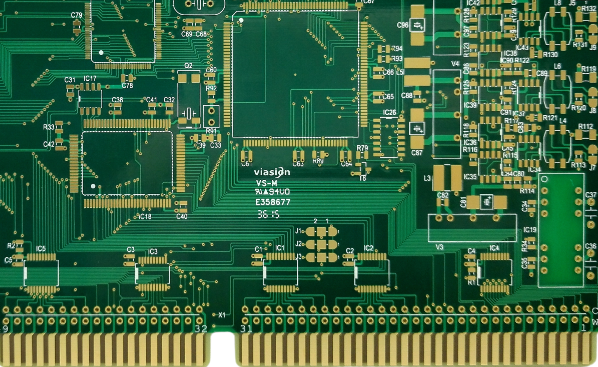
Modern layout tools are rule driven, so the rules have to be correct before the first trace is drawn. Set trace width, clearance, via size and plane clearance from the capability of the shop that will actually build the board.
Minimum values should be used only where they are needed. A design that runs everything at the process limit leaves no margin for adjustment, and the price of a panel rises sharply once the limits of the standard process are crossed. Our notes on designing for a standard process list the values most shops work to.
Importing the Netlist and Footprints
The netlist is the interface between the schematic and the layout. After it is imported, check that the part count matches the bill of materials and that every footprint has pad geometry that fits the package which will really be fitted.
Importing a revised netlist into a routed board is normal, but the update has to be done carefully. If the mechanical arrangement is already final, exclude the room regeneration step, otherwise the tool will rearrange components that were placed deliberately to satisfy the enclosure.
Component Placement
Placement decides most of the routing. Group the parts that belong to one function, keep the decoupling capacitor next to the pin it serves, and keep the high current path short and wide. The rest of the layout becomes easier once those clusters are right.
Leave room for the assembly process as well. Component placement has to respect the pick and place head, the reflow profile and rework access, so a part that is electrically allowed can still be a poor choice if nothing can reach it.
Routing the Outer Layers
Route the critical nets first: clocks, differential pairs, the switching nodes of a converter and any analogue signal that shares the board with digital logic. The order of routing should follow the electrical risk rather than the convenience of the drawing.
Keep the return path in mind for every trace. A signal that changes reference plane needs a stitching via beside the transition, and a trace routed over a plane gap behaves very differently from the simulation that assumed a solid plane underneath it.
Using the Inner Layers
On a four layer board the inner layers are usually solid planes, but splitting a plane into regions is common on mixed signal designs. A split plane is acceptable when the analogue and digital returns are separated and then joined at a single reference point.
Power distribution also benefits from the capacitance between the inner layers. The pair of copper planes forms a low inductance source for high frequency current, which is why a well built four layer stack often needs fewer bulk capacitors than the same circuit on two layers. Distribution practice is covered in our ground and power planning notes.
Stackup Symmetry and Material
The stackup has to be symmetrical about the centre line, including copper weights and dielectric thickness. An unbalanced build warps during reflow, and warpage then shows up as solder joint defects that are difficult to attribute to the stackup. See layer stackup for the standard builds.
Standard materials are adequate for most four layer work. Where the dielectric constant has to be tight, choose the material first and then design the trace geometry around its published values, including the frequency at which those values were measured.
Return Paths and Reference Integrity
Check the reference plane under every high speed net before the design is released. A layer change without a nearby ground via turns a controlled impedance trace into an antenna, and the effect is invisible in a static layout view.
The same discipline applies to connectors and cables. Signal pins that leave the board should be grouped with their returns, and the connector pinout should not force a signal to cross a plane boundary on the way to the outside world.
Design Review
A structured review catches more errors than any single automated check. Walk the schematic against the layout net by net for the critical circuits, then run the tool based checks for clearance, connectivity and unconnected copper. The escape and fanout rules are worth re-reading before a dense package is released.
Ask specifically about the items that tools cannot judge: current density in the power path, thermal spacing under the hot parts, test access and the mechanical fit. Those questions are cheap now and expensive after the panels have been etched.
Fabrication Outputs
Generate the Gerber data, the drill file, the stackup drawing and the fabrication notes from one frozen revision. Mixed revisions are the most common cause of a board that does not match its own documentation.
The notes should state the copper weight, the surface finish, the impedance targets and the tolerance that matters. Anything not written down will be produced to the shop default, and the default is chosen for the process rather than for the design.
First Article and Verification
The first panel is a measurement, not a formality. Check the conductor width and spacing, the annular ring, the finished hole size and the plating thickness on the coupon, then compare the result with the released values.
Impedance coupons are worth including on any board with controlled impedance. They let the shop verify the stackup with a time domain reflectometer before assembly, which is far cheaper than discovering a shift after the boards have been through reflow.
Keeping the Schedule Realistic
Most of the four layer pcb design process is spent on the decisions that precede routing. Library work, stackup selection and placement review take time, and compressing them usually moves the cost into rework at a later stage.
A short review at each stage is faster than one long review at the end. Freeze the schematic, the mechanical data and the stackup separately, and the layout can proceed while the next stage is still under discussion.
FAQ
Does a four layer board always need a ground plane on both inner layers? No, but the most predictable arrangement is one ground plane and one power plane. Splitting a plane into functional regions works when the returns are joined at a single reference point.
How wide should the power traces be? Wide enough that the temperature rise stays inside the design target. Use a current capacity table for the copper weight and the allowed rise, and keep the return path directly beneath the supply.
Can a two layer layout be upgraded to four layers later? It can, but the placement usually has to be revisited. The inner layers change the reference structure, so routing that was tuned for a two layer board is rarely optimal once planes are added.