PCB Shielding: EMI Protection, PCB Design & PCB Manufacturing Guide
The electronics supply chain involves multiple packaging and integration stages, ranging from semiconductor and component packaging to PCB assembly and finally to the enclosure or chassis. At every stage, electromagnetic compatibility (EMC) and electromagnetic interference (EMI) must be considered carefully.
During PCB Design and product development, EMI considerations have become an essential engineering requirement rather than an optional improvement. An individual electronic component may pass its required electrical tests when evaluated independently, yet the complete subsystem can still experience interference, signal degradation, or compliance failures after multiple components are integrated onto the same PCB.
The continuing miniaturization of electronic products has made this challenge even more significant. As component spacing, trace spacing, and overall system dimensions decrease, electromagnetic coupling between circuits can increase. At the same time, high-speed interfaces, switching power supplies, wireless communication circuits, processors, and RF devices can generate substantial amounts of electromagnetic noise.
If EMI problems are discovered late in the development cycle, manufacturers may face additional debugging, redesign, prototype fabrication, compliance testing, production delays, and customer complaints. Correcting an EMI problem after the PCB has already entered production can be significantly more expensive than preventing it during the initial design stage.
For this reason, effective PCB Shielding should be considered as early as possible through appropriate PCB layout, grounding, stackup design, component placement, and mechanical planning.
This guide explains what PCB shielding is, why EMI protection is important, the major shielding techniques, typical applications, and important considerations for PCB Manufacturing.
What Is PCB Shielding?
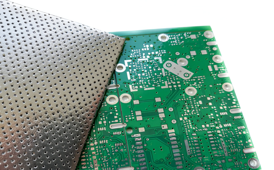
PCB Shielding is the use of conductive or electromagnetic barrier structures to reduce unwanted electromagnetic coupling between a PCB and its surrounding environment, or between different circuits on the same PCB.
EMI can travel through several coupling mechanisms, including:
- Conductive coupling
- Capacitive coupling
- Inductive coupling
- Radiated electromagnetic coupling
A circuit can both generate and receive electromagnetic interference. High-speed digital signals, switching regulators, clocks, motors, RF transmitters, and rapidly changing current paths are common sources of electromagnetic noise. Sensitive analog circuits, sensors, communication interfaces, and RF receivers may act as victims.
The purpose of shielding is therefore not simply to block external interference. A properly engineered shielding strategy should also limit the radiation generated by the PCB itself.
PCB shielding is only one level of a broader EMC strategy. Depending on the product architecture, engineers may use:
- Component-level shielding
- PCB-level shielding
- Cable and connector shielding
- Enclosure-level shielding
- Grounding and bonding
- Filtering
- Controlled PCB stackups
- Appropriate signal routing
For example, a conductive metal enclosure can provide a barrier against external electromagnetic fields, while a small EMI shield can isolate a sensitive RF or high-speed circuit directly on the PCB.
The most effective solution is usually a combination of circuit-level, PCB-level, and enclosure-level techniques rather than relying on a single shielding method.
Why Is PCB Shielding Important?
As electronic systems become smaller, faster, and more densely integrated, EMI control becomes increasingly important.
A modern PCB may contain processors, memory, wireless modules, switching power supplies, sensors, analog circuits, and high-speed communication interfaces within a very limited area. Without proper isolation and return-path control, these circuits can interact with one another through electromagnetic coupling.
EMI Suppression
The primary purpose of EMI Shielding is to reduce unwanted electromagnetic energy.
A shield can prevent external electromagnetic fields from coupling into sensitive circuits while also reducing radiation from noise-generating circuits. This is particularly important for wireless products, RF systems, high-speed digital electronics, and precision measurement equipment.
Improved Signal Integrity
Effective PCB shielding can contribute to better Signal Integrity by reducing unwanted coupling and crosstalk between adjacent circuits.
This becomes increasingly important as signal rise times become faster. Even when the fundamental clock frequency is relatively moderate, fast signal edges can contain significant high-frequency components.
Proper shielding should therefore be combined with:
- Controlled impedance routing
- Short signal paths
- Continuous reference planes
- Proper return paths
- Differential-pair routing
- Appropriate layer stackup
- Adequate spacing between noisy and sensitive circuits
Improved Reliability
EMI can cause intermittent malfunctions that are difficult to reproduce and diagnose. A product may operate correctly in a laboratory environment but fail when exposed to other electronic equipment, wireless signals, motors, switching power supplies, or other noise sources.
A well-designed shielding strategy can reduce these risks and improve the electromagnetic robustness of the final product.
Reduced Development and Production Costs
Addressing EMI problems during the initial PCB Design stage is generally more efficient than redesigning a PCB after compliance testing.
Late-stage EMI problems may require:
- PCB layout changes
- Additional prototypes
- Component substitutions
- Shield redesign
- Grounding modifications
- Additional filtering
- Repeated EMC testing
- Production delays
These activities can increase engineering and manufacturing costs significantly.
Regulatory and EMC Compliance
Electronic products may need to satisfy applicable EMC and EMI requirements depending on their industry, market, and intended application.
Relevant requirements may come from organizations and standards bodies such as IEC, CISPR, FCC, and other regional or industry-specific authorities. Automotive, aerospace, medical, industrial, and defense products can have additional requirements.
Pre-compliance testing during development can help identify potential EMI problems before formal certification testing.
Manufacturers should work with qualified testing laboratories and verify the requirements applicable to the specific product and target market.
What Are the Main PCB Shielding Techniques?
There is no single shielding method that works for every PCB. Engineers select the appropriate technique according to circuit frequency, noise level, board structure, available space, thermal requirements, mechanical constraints, and compliance targets.
1. Via Shielding
Via shielding, sometimes called a via fence, uses a series of closely spaced vias connected to a reference or ground plane.
These vias can be positioned around sensitive or high-frequency circuits to help control electromagnetic coupling and provide a more defined return-current path.
Via fences are commonly used around:
- RF circuits
- Antenna structures
- High-speed interfaces
- Sensitive analog circuits
- Isolated functional blocks
- Board edges
The spacing between shielding vias should be selected according to the relevant frequency range and PCB manufacturing capabilities.
Via shielding can also contribute to thermal conduction when appropriately connected to copper planes, although thermal management should be designed independently rather than assuming that a via fence alone will provide sufficient heat dissipation.
2. Stripline Routing
A Stripline PCB structure places a signal conductor between two reference planes within a multilayer board.
Because the signal is surrounded by reference planes, stripline routing can provide controlled electromagnetic fields and reduce coupling to neighboring circuits.
Stripline structures are especially useful for:
- High-speed digital signals
- RF circuits
- Controlled-impedance transmission lines
- Differential signals
- Noise-sensitive applications
The dielectric thickness and copper geometry between the reference planes must be controlled during PCB fabrication to achieve the intended impedance.
3. Ground Planes
A continuous Ground Plane is one of the most important elements of a low-noise PCB design.
A properly designed ground plane provides a low-impedance return path and can reduce unnecessary loop areas. It can also help establish a controlled electromagnetic environment around sensitive signal traces.
However, simply adding more copper does not automatically solve EMI problems. Engineers must understand current-return paths, layer transitions, plane discontinuities, and the relationship between signal routing and reference planes.
Poorly placed splits or gaps in a reference plane can force return currents to take longer paths, potentially increasing loop area and electromagnetic radiation.
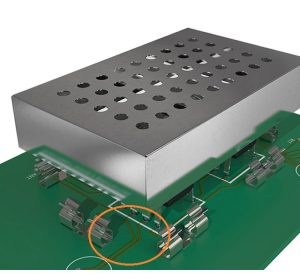
4. EMI Shield Cans and Shielding Enclosures
Physical EMI Shielding Cans are widely used to isolate specific circuits from electromagnetic interference.
A shield can is typically a conductive structure installed over an area of the PCB containing sensitive or noise-generating components.
Common configurations include:
- One-piece shield cans
- Two-piece shield systems
- Surface-mounted shield frames
- Removable shield covers
- Custom metal shielding structures
The PCB layout must account for the shield footprint, grounding points, mechanical clearance, component height, thermal requirements, and assembly process.
For automated PCB Assembly, shield structures should also be compatible with the manufacturer’s SMT or post-assembly process.
5. Conductive Coatings and Elastomeric Materials
Conductive coatings and conductive elastomers can be used at the enclosure or component-packaging level.
Conductive coatings may be applied to non-metallic surfaces to create an electromagnetic barrier. Conductive elastomers can provide both electrical conductivity and mechanical sealing around enclosure interfaces.
These materials are especially useful where mechanical openings, seams, connectors, or removable covers could otherwise create paths for electromagnetic energy to enter or escape.
PCB Shielding vs. Grounding: What Is the Difference?
PCB shielding and grounding are closely related but should not be treated as identical concepts.
Grounding primarily establishes electrical reference points and controlled return-current paths.
Shielding creates a physical or electromagnetic barrier that limits the transfer of electromagnetic energy.
A shield may need an appropriate connection to ground or chassis depending on its purpose and frequency range. However, simply connecting every conductive structure to the same ground without analyzing current paths can create unintended coupling or ground-loop problems.
Effective EMI control therefore requires coordinated decisions regarding:
- Signal routing
- Ground planes
- Chassis connections
- Shield termination
- Power distribution
- Cable routing
- Connector design
- PCB stackup
Applications of PCB Shielding
As electronic technology continues to expand into high-speed computing, wireless communication, automotive systems, medical equipment, and industrial automation, PCB shielding has become relevant to an increasingly broad range of applications.
Consumer Electronics
Smartphones, laptops, tablets, wearable devices, wireless routers, and other consumer products often contain multiple wireless and high-speed circuits operating within a small enclosure.
PCB shielding can help isolate RF circuits, processors, switching power supplies, and other noise-sensitive functional blocks.
Medical Electronics
Medical electronics often require stable and predictable electrical performance because inaccurate or unstable signals can affect monitoring and control functions.
Equipment such as patient monitoring systems, imaging equipment, diagnostic devices, and other medical electronics may incorporate shielding, filtering, grounding, and controlled PCB layouts as part of their EMC strategy.
For particularly sensitive medical applications, the entire system—including PCB, cables, sensors, enclosure, and external interfaces—may need to be evaluated as a complete electromagnetic system.
Telecommunications
Telecommunications equipment relies heavily on high-speed and high-frequency signal transmission.
PCB shielding can help reduce unwanted coupling between RF channels, digital processing circuits, power supplies, and communication interfaces. Proper impedance control and return-path design are equally important.
Automotive Electronics
Modern vehicles contain a growing number of electronic control units, sensors, cameras, wireless systems, power electronics, and communication networks.
Potential EMI sources include:
- Switching power converters
- Electric motors
- Ignition systems
- High-current power systems
- Wireless transmitters
- High-speed digital interfaces
Shielding and EMC-aware PCB Design can help improve electromagnetic robustness in these environments.
Aerospace and Defense Electronics
Aerospace systems can contain flight-control electronics, navigation equipment, communication systems, radar-related electronics, sensors, and other high-reliability systems.
Potential interference sources can include lightning, external radio-frequency systems, onboard transmitters, switching circuits, and other electronic subsystems.
For these applications, PCB shielding is typically only one part of a comprehensive EMC and electromagnetic-environment design strategy.
Industrial Automation
Industrial equipment can contain motors, variable-frequency drives, switching power supplies, sensors, PLCs, communication interfaces, and other potential EMI sources.
Shielding, grounding, filtering, and cable management can help maintain reliable operation in electrically noisy industrial environments.
PCB Design Considerations for EMI Shielding
The most cost-effective EMI strategy begins during the PCB design stage rather than after a prototype fails EMC testing.
Separate Noisy and Sensitive Circuits
High-noise circuits should be physically separated from sensitive analog, RF, sensor, and communication circuits whenever practical.
Examples of potential noise-generating circuits include switching regulators, motor drivers, clock generators, and high-speed processors.
Minimize Current Loop Areas
Large current loops can increase electromagnetic radiation and susceptibility.
Designers should keep high-frequency current paths short and provide appropriate return paths close to the associated signal paths.
Use Continuous Reference Planes
High-speed signals should generally have a continuous reference plane wherever possible.
Plane gaps, unnecessary layer transitions, and poorly positioned vias can disrupt return-current paths and increase EMI risk.
Optimize Component Placement
Component placement should follow the functional architecture of the circuit.
A practical approach is to organize the PCB into functional zones such as:
Power → Processing → High-Speed Interfaces → RF → Analog/Sensors → External Interfaces
The exact arrangement depends on the product architecture, but the objective is to prevent noisy circuits from unnecessarily crossing sensitive areas.
Plan the Shield Early
If a shield can or enclosure is required, its mechanical footprint should be incorporated into the PCB design from the beginning.
The designer should consider:
- Shield dimensions
- Shield mounting points
- Ground connections
- Component height
- Keepout areas
- Heat dissipation
- Assembly method
- Inspection requirements
- Serviceability
Adding a shield at the final stage can create mechanical and routing conflicts.
PCB Manufacturing Considerations for Shielding
A successful shielding design must also be manufacturable.
During PCB Manufacturing, manufacturers should consider:
- Layer registration
- Via positioning
- Copper thickness
- Dielectric thickness
- Controlled impedance
- Surface finish
- Solder mask clearance
- Shield mounting pads
- Mechanical tolerances
- Component clearance
- Lamination consistency
For high-frequency applications, even relatively small variations in PCB geometry can affect impedance and signal behavior.
For embedded or multilayer shielding structures, manufacturing tolerances become even more important.
A DFM review before production can help identify potential issues and reduce the risk of expensive redesigns.
How to Validate PCB Shielding Performance
PCB shielding should be verified through a combination of design analysis, prototype testing, and EMC measurements.
Common approaches include:
- Simulation and design review – Analyze signal paths, return paths, impedance, and potential coupling.
- PCB prototype testing – Evaluate the physical board under representative operating conditions.
- Pre-compliance EMC testing – Identify potential radiation or susceptibility problems before formal certification.
- Near-field probing – Locate areas of strong electromagnetic radiation on the PCB.
- Conducted-emission testing – Evaluate unwanted noise traveling through power or signal connections.
- Radiated-emission testing – Measure electromagnetic energy radiated by the product.
- Final compliance testing – Verify the finished product against the applicable regulatory or industry requirements.
Testing should be performed on the complete product configuration whenever possible because cables, connectors, enclosures, batteries, and other mechanical structures can significantly influence EMC performance.
How Kingda Can Support EMI-Aware PCB Manufacturing
For complex electronic products, EMI control should be considered throughout the complete development cycle rather than treated as a final testing problem.
Kingda can support customers by incorporating EMI-related considerations into PCB Design, fabrication, and assembly planning. Key areas may include multilayer stackup planning, grounding structures, controlled-impedance routing requirements, via structures, component placement, DFM review, and PCB assembly considerations.
For high-density or high-speed applications, early communication between the design team and PCB manufacturer can help identify manufacturability issues before prototype production.
This approach is particularly important when the product requires specialized PCB technologies, tight dimensional tolerances, high-frequency materials, HDI structures, or complex shielding configurations.
Conclusion
PCB shielding is an important part of modern electromagnetic compatibility engineering. As electronic devices become smaller, faster, and more densely integrated, the risk of electromagnetic coupling between components and circuits can increase.
Effective PCB Shielding can help reduce unwanted EMI, improve signal integrity, increase system robustness, and support regulatory compliance. However, shielding should not be viewed as an isolated solution.
A successful EMI strategy combines PCB Design, grounding, return-path control, stackup planning, component placement, signal routing, filtering, shielding structures, enclosure design, and appropriate EMC testing.
For manufacturers, addressing EMI during the earliest stages of design is generally more efficient than attempting to correct failures after production. By combining sound engineering practices with controlled PCB Manufacturing, manufacturers such as Kingda can help engineers develop compact, reliable, and EMC-conscious electronic products.