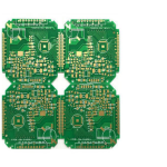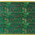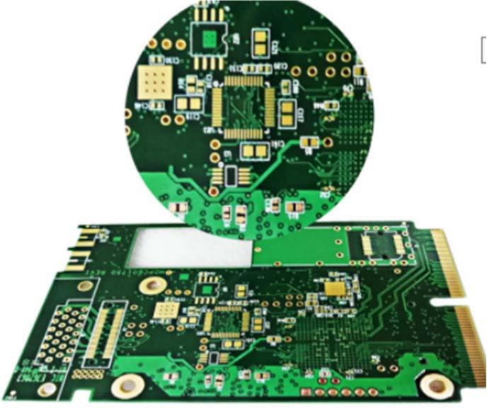
PCB Solder Mask is a critical part of modern PCB Manufacturing. It is a protective polymer coating applied to selected areas of a printed circuit board to protect exposed copper from oxidation, reduce the risk of solder bridging, and provide electrical insulation between adjacent conductive features.
The solder mask process becomes particularly important during assembly processes such as reflow soldering and wave soldering. During these processes, molten solder must be directed to specific pads and component terminals. The solder mask helps define the areas where solder is permitted to contact the PCB surface.
Although it is sometimes called a “solder resist” or simply “mask,” the term Solder Mask is more accurate because the material does not cover the entire PCB with solder. Instead, it selectively covers the board surface while leaving pads, test points, and other designated areas exposed.
What Is PCB Solder Mask?
A Solder Mask is generally a polymer-based coating applied over the copper circuitry of a PCB. After application and curing, it forms a protective insulating layer over the areas that do not need to be soldered.
Its primary functions include:
- Protecting exposed copper from oxidation and contamination
- Preventing accidental solder bridges
- Providing electrical insulation between adjacent conductors
- Improving resistance to environmental contamination
- Protecting copper traces from mechanical and chemical damage
- Helping define solderable pad areas during PCB assembly
- Improving the long-term reliability of the circuit board
Green is the most commonly used solder mask color, but black, blue, red, yellow, white, and other colors are also available depending on manufacturing and application requirements.
The color itself generally has less technical significance than the mask’s electrical, thermal, chemical, mechanical, and process characteristics.
Types of PCB Solder Mask
Different solder mask technologies are available for different PCB designs and production requirements. The most common categories include:
- Liquid Epoxy Solder Mask
- Liquid Photoimageable Solder Mask (LPSM)
- Dry Film Solder Mask (DFSM)
The appropriate technology depends on factors such as PCB geometry, surface topography, required registration accuracy, production volume, reliability requirements, and cost.
Liquid Epoxy Solder Mask
Liquid epoxy solder mask is one of the most basic solder mask technologies.
In this process, liquid epoxy-based material is applied to the PCB surface, commonly using screen printing or other coating methods. A screen or stencil controls where the material is deposited.
The epoxy material is then cured through a controlled thermal process.
The main advantages of liquid epoxy solder mask include:
- Relatively low manufacturing cost
- Simple application process
- Suitable for many conventional PCB designs
- Good protection for copper circuitry
- Compatibility with high-volume PCB production
However, compared with photoimageable processes, conventional screen-printed epoxy solder mask generally provides less precise control over very small openings and fine-pitch features.
For this reason, it is less suitable for some high-density PCB designs requiring extremely accurate solder mask registration.
Liquid Photoimageable Solder Mask (LPSM)
LPSM, or Liquid Photoimageable Solder Mask, is widely used for modern PCB production because it can provide much more accurate definition of solder mask openings.
The process generally involves coating the PCB with a liquid photoimageable material and then using an imaging process to selectively expose the required areas.
A typical LPSM process may include:
- PCB surface cleaning and preparation
- Application of the liquid photoimageable solder mask
- Pre-curing or drying
- Alignment with the solder mask image
- UV exposure
- Development
- Inspection
- Final curing
The imaging process defines the openings around pads, vias, test points, and other areas that must remain exposed.
Because the pattern is photographically defined, LPSM can achieve better registration and feature definition than basic screen printing.
It is therefore widely used for multilayer PCBs, fine-pitch components, BGA packages, HDI structures, and other high-density applications.
Dry Film Solder Mask (DFSM)
DFSM, or Dry Film Solder Mask, uses a pre-formed photosensitive film instead of a liquid coating.
The dry film is typically laminated onto the PCB surface under controlled pressure and temperature. Vacuum lamination can help achieve close contact between the film and the board while reducing trapped air and void-related defects.
The general process includes:
- PCB cleaning and surface preparation
- Dry-film solder mask lamination
- Photo exposure
- Development
- Inspection
- Final curing
One important advantage of DFSM is its ability to provide a relatively uniform film thickness over suitable board surfaces.
However, its performance depends strongly on PCB surface topography, copper features, lamination conditions, film characteristics, and process control.
LPSM vs. DFSM
Both LPSM and DFSM can use photoimaging technology, but their application methods are different.
| Feature | LPSM | DFSM |
|---|---|---|
| Material form | Liquid | Pre-formed dry film |
| Application | Coating, curtain coating, spray, or other processes | Lamination |
| Pattern definition | Photoimageable | Photoimageable |
| Thickness uniformity | Depends on coating process | Generally more uniform |
| Complex topography | Often more adaptable | Requires suitable surface conditions |
| Fine features | Suitable | Suitable |
| Process control | Requires coating and imaging control | Requires lamination and imaging control |
| Typical applications | General and high-density PCBs | Applications requiring controlled film thickness and specific surface conditions |
There is no universally superior solder mask technology. The selection should be based on PCB geometry, material stackup, feature density, assembly process, reliability requirements, and the manufacturer’s capabilities.
Top and Bottom Solder Mask
PCB design files normally distinguish between the solder mask on the top and bottom surfaces.
These are commonly referred to as:
- Top solder mask
- Bottom solder mask
These terms describe the physical location of the solder mask layer rather than a particular material or manufacturing technology.
A PCB may therefore use LPSM, DFSM, or another suitable solder mask technology on either surface depending on the manufacturing process.
Solder Mask Application and Curing
Regardless of the selected PCB Solder Mask technology, surface preparation is critical.
Before applying the solder mask, the PCB surface must be properly cleaned to remove contaminants such as:
- Dust
- Oil
- Fingerprints
- Chemical residues
- Oxidation products
- Particles from previous processes
Poor surface preparation can reduce adhesion and may lead to defects such as peeling, blistering, pinholes, or contamination beneath the solder mask.
After application and imaging, the solder mask undergoes the appropriate curing process.
For conventional epoxy systems, thermal curing is commonly used. Photoimageable systems generally require UV exposure to define the image, followed by additional thermal curing according to the material manufacturer’s process specifications.
The exact curing profile depends on the solder mask material and supplier requirements.
PCB Solder Mask Openings
A key function of the solder mask is to determine which areas remain exposed for soldering or electrical testing.
Typical exposed features include:
- Component pads
- BGA pads
- Connector contacts
- Test points
- Selected vias
- Other designated copper features
The opening must be sufficiently large to compensate for manufacturing registration tolerances while still providing adequate isolation between adjacent conductors.
For fine-pitch components, solder mask registration becomes increasingly important because even a small alignment error can reduce pad clearance or create a risk of solder bridging.
Solder Mask Defined and Non-Solder Mask Defined Pads
For some fine-pitch applications, PCB designers must distinguish between solder-mask-defined (SMD) and non-solder-mask-defined (NSMD) pads.
In an NSMD structure, the solder mask opening is larger than the copper pad, leaving the copper pad boundary defined primarily by the copper pattern.
In an SMD structure, the solder mask opening is intentionally smaller than the copper feature, allowing the solder mask to define part of the pad boundary.
The appropriate structure depends on component package requirements, pad geometry, solder joint reliability, PCB fabrication capability, and assembly requirements.
Therefore, designers should follow the component manufacturer’s recommendations and communicate critical requirements with the PCB manufacturer.
How Thick Should PCB Solder Mask Be?
Solder Mask Thickness is not a universal fixed value.
The actual thickness depends on:
- Copper thickness
- Surface topography
- Solder mask material
- Application method
- PCB design
- Required electrical insulation
- Component pitch
- Surface finish
- Manufacturing process
A flat laminate area may have a different solder mask thickness from an area containing dense copper traces, pads, or other surface features.
For this reason, a nominal solder mask thickness should always be specified and controlled according to the relevant material specification and manufacturer’s process capability rather than treating one thickness value as suitable for every PCB.
For demanding applications, designers should discuss minimum and maximum solder mask thickness requirements with the PCB manufacturer.
PCB Surface Finish and Solder Mask
The Surface Finish protects exposed copper areas that are intentionally left open after solder mask application.
Common PCB surface finishes include:
- HASL
- Lead-free HASL
- ENIG
- ENEPIG
- Immersion tin
- Immersion silver
- OSP
The solder mask and surface finish perform different functions.
The solder mask protects selected areas of the PCB surface, while the surface finish protects exposed copper pads and provides an appropriate surface for soldering, wire bonding, or other assembly requirements.
For example, ENIG is commonly used for fine-pitch and high-density applications because it provides a relatively flat solderable surface.
The appropriate Surface Finish depends on the PCB application, assembly process, component requirements, environmental conditions, reliability expectations, and cost.
Solder Mask and Reflow Soldering
During reflow soldering, solder paste is deposited onto designated PCB pads and then heated according to a controlled temperature profile.
The PCB Solder Mask helps prevent solder from spreading onto adjacent copper areas.
Solder mask quality can therefore influence:
- Solder bridging
- Solder ball formation
- Pad definition
- Surface insulation
- Assembly yield
- Long-term reliability
However, solder mask alone does not determine reflow quality. Solder paste formulation, stencil design, pad geometry, component placement, reflow profile, PCB surface finish, and assembly equipment also play important roles.
Solder Mask Design Guidelines
When designing the solder mask layer, PCB designers should consider the actual manufacturing capability rather than applying a single universal clearance value.
Important design factors include:
- Solder mask registration tolerance
- Pad-to-mask clearance
- Minimum solder mask web
- Component pitch
- Via size
- Via-to-pad spacing
- Copper thickness
- Board surface topography
- Manufacturing tolerances
For example, very narrow solder mask webs between adjacent pads may become difficult to manufacture consistently. If the clearance is too small, neighboring openings can merge.
Similarly, excessive solder mask expansion can reduce the isolation distance between adjacent pads.
The appropriate solder mask expansion and web width should therefore be defined according to the PCB manufacturer’s design rules.
How to Add Solder Mask in PCB Design
In PCB CAD software, the solder mask is normally represented as dedicated top and bottom solder mask layers.
When preparing manufacturing data, these layers are typically exported as separate files, commonly as Gerber or another supported manufacturing-data format.
The designer should verify:
- All required pads have correct solder mask openings.
- Unwanted copper is properly covered.
- Fine-pitch pads have sufficient solder mask clearance.
- Via openings are correctly defined.
- Test points are accessible where required.
- Solder mask expansion follows the manufacturer’s capabilities.
- Top and bottom solder mask data are correctly aligned.
- No accidental mask slivers or merged openings exist.
A final DFM review is strongly recommended before releasing the design for production.
Common PCB Solder Mask Defects
Improper process control can result in several solder mask defects.
Pinholes
Small holes in the solder mask can expose copper and reduce surface protection.
Blisters
Poor adhesion or trapped contamination can result in blistering during subsequent thermal processes.
Peeling
Insufficient surface preparation or inadequate curing may cause the mask to detach from the PCB surface.
Misregistration
If the solder mask image is not accurately aligned with the copper pattern, openings may be shifted relative to the pads.
Solder Mask Bridging
If adjacent mask openings are too close or the process is not properly controlled, the intended separation between openings may not be maintained.
Incomplete Curing
Insufficient curing can affect the mechanical, chemical, and thermal performance of the solder mask.
These defects can be reduced through appropriate material selection, surface preparation, imaging, curing, inspection, and process control.
Choosing the Right PCB Solder Mask
The appropriate PCB Solder Mask should be selected according to the complete application rather than simply choosing the lowest-cost option.
For standard electronic products, conventional liquid solder mask may provide an economical and reliable solution.
For high-density or fine-pitch designs, photoimageable systems such as LPSM may provide better pattern definition and registration.
For applications requiring controlled film thickness and suitable surface characteristics, DFSM may also be considered.
For aerospace, automotive, medical, telecommunications, and other high-reliability applications, designers should additionally consider:
- Thermal cycling
- Chemical resistance
- Moisture resistance
- Electrical insulation
- Adhesion
- Flame-retardant requirements
- Long-term reliability
- Applicable industry standards
The final selection should be made together with the PCB manufacturer and, where applicable, the solder mask material supplier.
Kingda’s PCB Solder Mask Manufacturing
At Kingda, PCB Manufacturing is approached as an integrated process in which solder mask performance is considered together with PCB materials, copper patterns, surface finish, drilling, lamination, and assembly requirements.
For high-density PCBs, accurate solder mask imaging and registration are particularly important. The manufacturing process must account for board expansion, copper distribution, surface topography, material characteristics, and process tolerances.
Kingda can evaluate solder mask requirements during the DFM stage and help customers select an appropriate manufacturing process based on PCB structure, feature density, surface finish, assembly technology, and application requirements.
This approach helps balance solderability, electrical insulation, manufacturing yield, reliability, and overall production cost.
Conclusion
PCB Solder Mask is much more than a colored coating on a circuit board. It is an important functional layer that protects copper, controls soldering areas, improves electrical insulation, and contributes to the reliability of the finished PCB.
Liquid epoxy, LPSM, and DFSM provide different solutions for different PCB structures and manufacturing requirements. The correct choice depends on board geometry, feature density, surface topography, required registration accuracy, reliability requirements, assembly technology, and production cost.
At the design stage, engineers should pay close attention to solder mask openings, mask expansion, minimum mask web, pad geometry, via treatment, and manufacturer-specific DFM rules.
By coordinating PCB Design and PCB Manufacturing requirements from the beginning, manufacturers and designers can achieve better solderability, higher production yield, and more reliable electronic products.