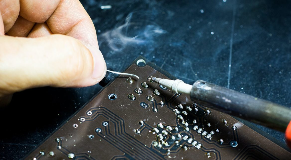
PCB Thermal Design: Keeping Component Temperatures Under Control
Heat is the quiet failure mode of modern electronics. A board that passes every electrical test on the bench can still fail in the field because a regulator, a power amplifier or an FPGA runs hot enough to shorten its own life and the life of the parts around it. PCB thermal design is the discipline of giving that heat somewhere to go. It starts with understanding how heat moves through copper, laminate and air, and it ends with numbers that can be verified on a thermal camera during qualification testing.
Where the Heat Goes
Heat leaves a component by three routes at once: conduction through the leads and the copper beneath them, convection into the surrounding air, and radiation from hot surfaces. Inside a sealed enclosure with still air, conduction does most of the work, which is why copper area matters far more than airflow in compact products. Convection becomes significant only when there is a genuine air path, and radiation matters mainly once surface temperatures climb well above ambient.
Temperature rise is never uniform. A board can have a small hot spot under a power device and a wide warm area spread across a plane, and the two need different fixes. Measuring the surface with a thermal camera before changing anything shows which case applies. Local heating usually calls for more copper and vias directly under the part, while broad warming suggests that the whole board is short of spreading area or that the enclosure has no usable path to the outside.
Copper Pour, Planes and Spreading Area
Copper is the best thermal conductor already present in the design. A generous copper pour connected to the device ground pad spreads heat laterally far better than the laminate ever could, because FR-4 conducts heat roughly a thousand times less effectively than copper. Connect the pour to the thermal pad of the hot device with a short, wide path, and avoid thin necks and narrow traces that create a bottleneck exactly where the heat needs to leave.
Where a copper pour is used, tie it to the plane with a via fence so that heat has a vertical path as well as a lateral one. Several layers of copper joined by vias behave like a single thicker conductor, and the improvement is often larger than designers expect. Traces feeding the hot device should be sized for heat as well as for voltage drop, which is where trace width and current calculation becomes a thermal exercise rather than only an electrical one.
Thermal Via Arrays Under Power Devices
A thermal via is simply a plated hole used to move heat rather than current. An array of small vias under a QFN or BGA thermal pad transfers heat to inner planes and to the opposite side of the board, where a larger copper area can dissipate it. Vias placed only under the centre of the pad certainly help, but a ring around the pad perimeter is often more effective, because the heat has already spread sideways by the time it reaches the middle.
Diameter and plating thickness matter less than the total copper cross section and the quality of the connection to a plane. Solder wicking through open vias is the usual worry, so many designs specify tented or plugged vias across the pad area. Our comparison of thermal via versus filled via construction explains when each approach justifies the extra process step and when a plain array is enough.
Heat Sink, Pads and Interface Materials
A heat sink only helps if heat can actually reach it. The path from the die to the sink includes the package, the solder joint, the board, the thermal pad and the mounting hardware, and any weak link in that chain sets the temperature. A small sink bonded through a thick, poorly applied interface layer can perform worse than no sink at all, because the added thermal resistance outweighs the extra surface area it provides.

Thermal pads and gap fillers are the practical choice when a metal enclosure or a sink has to contact components of uneven height. Choose a pad thick enough to compress properly, because a pad that barely touches transfers almost nothing, and remember that repeated thermal cycling relaxes the contact over time. Where the sink is bolted through the board, keep the mounting force even and avoid loading the solder joints of the component being cooled.
Placement: Keeping Heat Sources Apart
Two hot components placed side by side raise each other’s temperature even though neither is faulty. Spread the main heat sources across the board, keep temperature sensitive parts such as crystals, sensors and electrolytic capacitors away from them, and place the components that tolerate heat between the sources and the sensitive ones. Orientation matters too: mounting a board vertically in a freely convecting enclosure usually beats a horizontal layout, because the chimney effect keeps air moving.
Grouping is not always possible on a dense board, and where components must cluster, give the cluster a dedicated copper area and a clear path toward the enclosure wall. Splitting power nets to separate the hot, noisy supply of a switching stage from the clean supply of an analogue front end also helps here, as described in power plane splitting rules. The aim is to keep the thermal map and the electrical map of the board pointing in the same direction.
Material, Stackup and Copper Weight
Standard FR-4 is an electrical insulator and a poor thermal conductor, and its thermal conductivity falls as resin content rises. Higher copper weight, thicker inner layers and metal backed substrates all improve spreading. Aluminium and ceramic substrates move heat far better than FR-4 but change the manufacturing route, so they are reserved for boards where the thermal problem is genuinely severe rather than merely inconvenient.
Stackup decisions interact with everything else. Putting the ground plane directly under the component side shortens the vertical heat path, and using two ounces of copper on the outer layers is a cheap upgrade compared with moving to a metal substrate. The trade-offs between base materials are covered in our comparison of FR-4 and G-10 laminate, and the same reasoning about resin content and thermal path applies to the higher performance laminates.
Estimating Junction Temperature Before You Build
Junction temperature is the number that matters, and it can be estimated long before a prototype exists. Start with the ambient inside the enclosure rather than room temperature, add the temperature rise of the board, and add the rise across the package from the thermal resistance quoted in the data sheet. Compare the result with the rated maximum and keep a margin, because airflow assumptions and interface quality in production are rarely as good as they are on the bench.
After the first build, verify the estimate with a thermal camera or with thermocouples under the worst case load and the worst case ambient. If the measurement disagrees with the calculation, the interface material or the airflow path is usually responsible. Recording the measured values in the design file makes the next product faster to develop, because the assumptions no longer have to be rebuilt from scratch.
FAQ
How much copper area does a hot component need? There is no single number, because the answer depends on the power dissipated, the permitted temperature rise and the airflow. A practical approach is to start with a pour several times the area of the thermal pad on both sides of the board, connect the layers with a via array, then measure. Add area until the measured temperature rise falls inside the margin.
Are thermal vias always necessary? No. For a device dissipating a fraction of a watt into a large copper area, a pour on the component side is often enough. Thermal vias earn their place when heat has to reach inner planes or the opposite side of the board, or when the copper available on the component side is limited by routing density. The determining factor is the vertical heat path, not habit.
Can a heatsink rescue a badly laid out board? Rarely. A sink lowers the resistance from the package to the air, but it cannot compensate for a constricted path inside the board or a poor interface layer. If the copper under the device is thin and the pad never fully compresses, fitting a bigger sink changes very little. Fix the conduction path first, then size the sink against what remains.