Thermal Via Design Guide
A thermal via is a plated hole whose purpose is to carry heat rather than current. It connects a hot component to an internal or a bottom layer that can spread the heat into a larger area, and it is the cheapest thermal improvement available to a board designer. The difficulty is that the amount of heat a via can carry is modest, so the value comes from the array rather than from any single hole, and the array interacts with the assembly process.
What a Via Can Do
Copper has a thermal conductivity several hundred times that of the resin in a laminate, so a plated hole is a low resistance path through the thickness of the board. The resistance is set by the copper cross section, which is the circumference of the barrel multiplied by its plating thickness.
That cross section is small. A 0.3 mm hole with a 25 micron plating has a copper area of roughly one twentieth of a square millimetre, which is comparable to a short trace. A single via therefore carries a modest amount of heat, and a realistic design uses an array of tens of holes.
The value of the array is not only the sum of the individual paths. The vias are connected to a copper area on the other side, and that area spreads the heat laterally into a region much larger than the component footprint, which lowers the temperature of the whole assembly rather than just the joint.
Via Geometry
The diameter should be as small as the drilling process allows, because a smaller hole leaves more copper area on the pad itself and allows a tighter pitch. The plating thickness should be at the top of the specification, since the thermal resistance is inversely proportional to it.
The pitch is a compromise between thermal performance and assembly. A tighter pitch lowers the thermal resistance of the array but removes copper between the holes, and past a certain point the pad becomes a lattice of thin webs that the paste cannot bridge reliably.
Filled and capped vias remove the assembly problem entirely. A via that is filled with a conductive or a non conductive plug and capped with copper gives a flat pad that prints like a solid surface, at the cost of an extra process step and a stricter specification on the fill quality.
Heat Spreading and Heat Removal
It is worth separating the two functions. A via array that ends on an internal plane spreads the heat sideways and lowers the local temperature, but the heat stays in the board and must eventually leave through the surface. That is heat spreading.
A via array that ends on a bottom layer with its own copper area, or on a metal core or a heat sink, removes the heat from the board. That is heat removal, and it is the function that matters when the total power is high rather than when a single point is hot.
The design should state which of the two is intended. A board that relies on removal through the underside needs the bottom copper to be continuous and the assembly to leave that face clear of other components, and a design that only spreads heat is usually adequate for a small package with a moderate load.
Plating and Reliability
The plating inside a thermal via has to survive the assembly and the service life. A thin or incomplete barrel has a higher thermal resistance, and it also has a higher chance of cracking under thermal cycling, because the barrel sees the full expansion of the board thickness.
Vias in a thermal pad are often placed in a large area of copper, which changes the plating current distribution and can leave the barrels thinner than the specification. The plating thickness should be verified on a coupon or by a section rather than assumed from the surface.
Where the assembly will be thermally cycled, a filled via is more reliable than an open one, because the plug supports the barrel and removes the void that would otherwise concentrate the strain. The extra cost is small compared with the cost of a field failure in a power device.
Assembly Problems
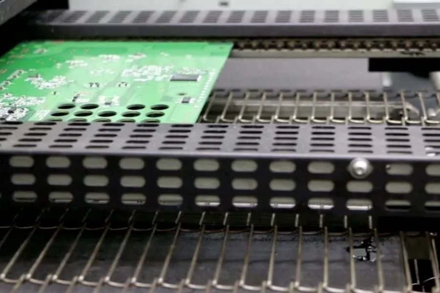
An open via in a solder pad wicks solder away from the joint during reflow. The solder flows into the barrel and out of the joint, which leaves a starved fillet on the surface and a void in the thermal interface. The defect is often described as wicking and it is the most common reason to fill and cap a via array.
Voids in the solder interface are the second problem. Each open via is a place where the paste does not bond to the pad, and the void content of a power device attach can rise enough to affect the thermal path that the vias were added to improve.
Outgassing from a plated through hole during reflow produces a blowhole that pushes solder out of the joint. The effect is worse when the board has absorbed moisture, so the baking schedule and the storage of the panels are part of the thermal design rather than a separate housekeeping detail.
Design and Verification
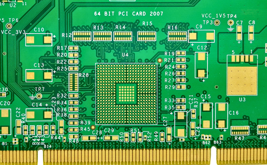
The array should be placed under the thermal pad of the package and extended slightly beyond it, so that the copper on the far side has a larger area than the component. The internal plane or the bottom copper that the vias connect to must be solid in that region, with no slots or splits that would block the lateral spread.
The thermal performance should be estimated before the layout is finished, with a simple calculation for the via array and a simulation for the assembly where the power is significant. The estimate is not a substitute for measurement, but it identifies the cases where the array is doing nothing.
Verification is by measuring the case temperature of the device under load, with the board in the enclosure and at the worst ambient. A bench measurement in free air will show a thermal path that the product does not have, and the difference is often the entire margin.
Practical Rules
Use many small vias with good plating rather than a few large ones, connect them to a solid copper area, and decide whether the design spreads heat or removes it. Where solder wicking is a risk, fill and cap the vias.
Record the via geometry and the plating with the build records and pair the array with the thermal design rules and the hole copper specification so that the barrels are built as the thermal calculation assumed.
FAQ
How many thermal vias are enough? It depends on the power and the copper area they connect to. Each via carries a modest amount of heat, so a realistic design uses an array of tens of holes rather than a few.
Why fill and cap a thermal via? An open via wicks solder out of the joint during reflow and leaves a void in the thermal interface. Filling and capping gives a flat, printable pad.
What is the difference between spreading and removal? Spreading lowers the local temperature by moving heat sideways in the board. Removal takes the heat out of the board, and it needs a copper area or a heat sink on the far side.