In modern electronics manufacturing, the performance, reliability, and service life of a finished product are closely related to PCBA quality control. Even a small defect, such as a soldering crack, component misalignment, incorrect component value, solder bridge, or hidden BGA soldering issue, can lead to intermittent failures, costly rework, product recalls, and field failures.
High-quality PCBA testing is therefore not a single inspection performed at the end of production. Instead, it is a systematic quality assurance process that begins with incoming materials and continues through PCB fabrication, component placement, soldering, inspection, electrical testing, and final functional verification.
For high-density and complex electronic products, manufacturers need a comprehensive PCBA inspection strategy combining automated inspection equipment, electrical testing, process monitoring, and engineering expertise.
As an experienced PCB manufacturer and PCB assembly service provider, Kingda provides PCB prototype manufacturing, rapid PCB prototyping, SMT assembly, through-hole assembly, and comprehensive PCBA testing to support customers from initial design verification through volume production.
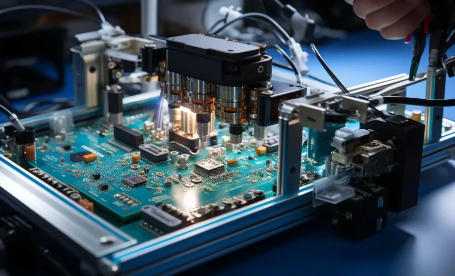
This guide explains the major PCBA testing methods, inspection stages, quality standards, and testing considerations that engineers should understand when developing reliable electronic products.
What Is PCBA Testing?
PCBA testing is the systematic process of inspecting, measuring, and validating a printed circuit board assembly to confirm that the assembled board meets its electrical, mechanical, functional, and quality requirements.
A complete PCBA inspection process may include:
- Incoming Quality Control (IQC)
- Bare PCB inspection
- Component verification
- Solder Paste Inspection (SPI)
- Automated Optical Inspection (AOI)
- Automated X-Ray Inspection (AXI)
- Visual inspection
- Flying Probe Testing (FPT)
- In-Circuit Testing (ICT)
- Functional Circuit Testing (FCT)
- Electrical safety testing
- Final inspection and traceability verification
Each method detects different types of defects. Therefore, relying on only one inspection technology cannot provide comprehensive quality assurance for complex PCB assemblies.
A typical quality workflow can be summarized as:
Incoming Material Inspection → PCB Inspection → SPI → SMT Placement → AOI → Reflow Soldering → X-Ray Inspection → Electrical Testing → Functional Testing → Final QC → Shipment
At Kingda, inspection and testing are integrated into the manufacturing process rather than being treated as an isolated final-stage activity.
PCBA Testing Before Assembly
Effective PCBA quality control starts before components are placed on the PCB. Incoming materials must be verified to prevent defective, incorrect, damaged, or counterfeit materials from entering production.
1. Incoming Quality Control (IQC)
Incoming Quality Control is the first major checkpoint in the PCBA manufacturing process.
The inspection normally covers components, bare PCBs, solder paste, and other production materials.
Component Verification
Components should be checked against the approved Bill of Materials (BOM) and engineering documentation.
Typical checks include:
- Manufacturer part number
- Component value
- Package type
- Tolerance
- Quantity
- Manufacturer information
- Date code and lot information
- Packaging condition
- Moisture Sensitivity Level (MSL)
- RoHS and other applicable compliance requirements
Incorrect component values can cause immediate circuit malfunction, while counterfeit or substandard components may result in intermittent failures or reduced product life.
For critical components, additional verification methods may be required depending on the application.
Moisture Sensitivity Level Management
Many semiconductor packages and some passive components can absorb moisture during storage.
If moisture-sensitive components are exposed beyond their specified floor life, moisture may vaporize rapidly during reflow soldering. This can result in package cracking, delamination, internal damage, or the phenomenon commonly known as popcorning.
Proper MSL management therefore includes:
- Checking MSL classification
- Verifying dry-pack integrity
- Recording exposure time
- Controlling storage conditions
- Baking components when required
- Maintaining material traceability
Kingda incorporates material verification and storage management into its PCBA quality control workflow to reduce material-related manufacturing risks.
Bare PCB Inspection Before PCBA
Before components are mounted, the bare PCB should undergo appropriate inspection to ensure that its physical and electrical characteristics meet the design requirements.
Visual Inspection
Visual inspection can identify:
- Scratches
- Contamination
- Copper exposure
- Oxidation
- Solder mask defects
- Surface damage
- Poor plating
- Silkscreen errors
Dimensional Inspection
Critical PCB dimensions should be verified, including:
- Board length and width
- Board thickness
- Hole diameter
- Connector locations
- Slot dimensions
- Edge clearance
- Warpage and twist
Excessive PCB warpage can negatively affect solder paste printing and component placement, particularly on large or thin boards.
Electrical Testing
Electrical testing, commonly referred to as E-Test, verifies the connectivity of the PCB.
Depending on production volume and product requirements, manufacturers may use:
- Flying probe testing
- Bed-of-nails testing
- Dedicated electrical test fixtures
The objective is to detect:
- Open circuits
- Short circuits
- Incorrect connections
- Manufacturing defects in conductive paths
Solder Mask and Silkscreen Inspection
Solder mask registration and silkscreen alignment should also be checked.
Poor solder mask registration can contribute to solder bridging, while incorrectly positioned silkscreen markings can interfere with component identification or manual assembly.
PCBA Inspection During SMT Assembly
Once incoming materials have passed inspection, the focus shifts to controlling the assembly process.
This stage is particularly important because many SMT defects originate during solder paste printing and component placement.
1. Solder Paste Inspection (SPI)
Solder Paste Inspection (SPI) is one of the most important inspection methods in modern SMT assembly.
SPI equipment measures solder paste deposits before components are placed on the PCB.
Modern 3D SPI systems can measure:
- Solder paste volume
- Solder paste height
- Solder paste area
- X/Y offset
- Deposit shape
- Printing consistency
These measurements help identify problems such as:
- Insufficient solder paste
- Excessive solder paste
- Misaligned deposits
- Bridging
- Missing solder paste
- Inconsistent printing
Because solder paste printing directly affects solder joint quality, SPI allows manufacturers to identify process drift before it becomes a large-scale production problem.
For high-density PCB assemblies, accurate SPI control becomes particularly important because fine-pitch components and small packages have much narrower process tolerances.
2. Automated Optical Inspection (AOI)
Automated Optical Inspection (AOI) uses cameras and image-processing technology to inspect assembled PCBs.
AOI can be performed at different stages of production.
Pre-Reflow AOI
Pre-reflow inspection can identify:
- Missing components
- Incorrect components
- Component misalignment
- Polarity errors
- Component orientation errors
- Tombstoning
- Placement defects
Finding defects before reflow makes correction and rework easier.
Post-Reflow AOI
Post-reflow AOI inspection focuses on soldering and component-placement quality.
It can detect:
- Solder bridges
- Insufficient solder
- Excess solder
- Lifted leads
- Missing components
- Misaligned components
- Incorrect polarity
- Soldering abnormalities
However, AOI has an important limitation: it primarily examines visible surfaces.
It cannot reliably inspect solder joints hidden underneath packages such as:
- BGA
- QFN
- LGA
- Bottom-terminated components
This is where X-Ray inspection becomes necessary.
3. Automated X-Ray Inspection (AXI)
Automated X-Ray Inspection (AXI) is used to inspect hidden solder joints and internal structures that cannot be evaluated through conventional optical inspection.
X-Ray inspection is especially useful for:
- BGA solder balls
- QFN thermal pads
- LGA connections
- Hidden solder joints
- Voids
- Opens
- Shorts
- Insufficient solder
- Component alignment
One important application is void inspection.
Gas trapped within a solder joint can form voids. Excessive voiding may affect thermal transfer, electrical performance, and mechanical reliability depending on the component and application.
For power electronics, high-density assemblies, and BGA-based designs, X-Ray inspection can provide important information that AOI alone cannot obtain.
Kingda can incorporate X-Ray inspection into the PCBA quality process when the component structure, product reliability requirements, or customer specifications require hidden-joint inspection.
PCBA Testing After Reflow
After soldering, the assembled PCB enters a more comprehensive inspection and validation stage.
The objective is not only to confirm soldering quality but also to verify electrical connectivity and product functionality.
Visual Inspection and IPC Standards
Automated inspection systems provide extensive coverage, but professional visual inspection remains an important part of PCBA quality control.
Inspectors may examine:
- Solder joints
- Component orientation
- PCB contamination
- Mechanical damage
- Connector installation
- Component markings
- Solder bridges
- Excess solder
- Missing components
- Manufacturing workmanship
For electronic assemblies, IPC-A-610 is one of the major industry references used to evaluate assembly acceptability.
IPC-A-610 defines different product classes according to the intended application and reliability requirements.
Class 1
General electronic products where the primary requirement is basic functionality.
Class 2
Dedicated service products where continued performance and extended service life are important.
Class 3
High-performance or harsh-environment products where continuous performance and reliability are critical.
The appropriate acceptance criteria should always be determined according to the customer’s product requirements, applicable standards, and intended operating environment.
Flying Probe Testing (FPT)
Flying Probe Testing (FPT) is particularly suitable for prototypes, engineering samples, and low-volume PCB assembly.
Instead of using a dedicated fixture, movable probes contact predefined test points on the PCB.
Flying probe testing can verify:
- Open circuits
- Short circuits
- Electrical connections
- Certain component values
- Polarity
- Basic circuit characteristics
Advantages of Flying Probe Testing
- Low fixture investment
- High flexibility
- Suitable for prototypes
- Suitable for low-volume production
- Easy to adapt to design revisions
The main limitation is testing speed. Because the probes move individually between test points, cycle time can be longer than fixture-based ICT for high-volume production.
For PCB prototype manufacturing and low-volume PCBA projects, however, flying probe testing can provide an efficient testing solution without the cost of a dedicated fixture.
In-Circuit Testing (ICT)
In-Circuit Testing (ICT) is commonly used for mature products and higher-volume production.
ICT uses a dedicated fixture containing multiple test probes that contact designated test points on the PCB.
It can evaluate:
- Component values
- Opens
- Shorts
- Component orientation
- Electrical connectivity
- Certain analog and digital parameters
ICT Advantages
- High testing speed
- Repeatable test results
- Good manufacturing defect coverage
- Suitable for stable high-volume products
- Efficient for repetitive production
The main consideration is the initial cost of developing a dedicated test fixture.
Therefore, ICT is generally more appropriate when production volume is sufficient to justify the fixture investment.
Functional Circuit Testing (FCT)
Functional Testing (FCT) evaluates whether the assembled PCB actually performs its intended functions.
Unlike inspection systems that primarily look for manufacturing defects, FCT evaluates the behavior of the completed circuit.
Depending on the product, FCT may verify:
- Power-up behavior
- Communication interfaces
- Sensor signals
- Display operation
- LED operation
- Motor control
- Wireless communication
- Analog outputs
- Digital outputs
- Protection functions
For example, a completed control board may need to communicate with a sensor, activate an output, transmit data, and respond correctly to external commands.
If all required functions operate according to the product specification, the board passes the functional test.
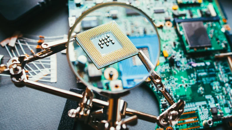
AOI vs X-Ray vs ICT vs FCT
Different PCBA testing methods address different types of manufacturing and functional risks.
| Testing Method | Main Purpose | Typical Defects Detected | Typical Application |
|---|---|---|---|
| SPI | Solder paste verification | Insufficient/excess paste, offset, volume variation | SMT assembly |
| AOI | Surface inspection | Misplacement, polarity, solder bridges, missing parts | SMT/PCBA |
| AXI | Hidden-joint inspection | BGA defects, voids, hidden solder issues | High-density PCBA |
| FPT | Electrical connectivity | Opens, shorts, selected component faults | Prototype/low volume |
| ICT | Component and circuit verification | Component values, opens, shorts | Medium/high volume |
| FCT | Functional verification | System-level functional failures | Finished PCBA |
The key point is that these technologies are complementary rather than interchangeable.
For example, FCT cannot replace AOI because a board can sometimes pass its functional test while still containing workmanship defects that could reduce long-term reliability.
Similarly, AOI cannot replace X-Ray when solder joints are hidden beneath BGA or QFN packages.
How Kingda Builds a Complete PCBA Quality Control System
As an experienced PCB manufacturer and PCB assembly service provider, Kingda integrates quality control throughout the manufacturing process.
Our approach covers the complete production chain:
PCB Fabrication → Incoming Inspection → SMT Assembly → SPI → AOI → Reflow → X-Ray When Required → DIP/THT Assembly → Electrical Testing → Functional Testing → Final QC → Packaging & Traceability
This integrated approach allows potential problems to be identified earlier rather than waiting until final inspection.
1. Engineering and DFM Review
Before production, engineers can review PCB designs for potential manufacturing problems.
Typical considerations include:
- Component spacing
- Pad design
- Solder mask clearance
- Via placement
- Component orientation
- Assembly accessibility
- Thermal considerations
- Test-point availability
- SMT and THT process requirements
Early DFM engineering review can reduce manufacturing risks and unnecessary redesign.
2. PCB Manufacturing
Kingda supports customers from prototype development through production manufacturing.
As a PCB manufacturer, Kingda can coordinate PCB fabrication and PCBA production to help maintain consistency between the board design and assembly process.
3. SMT and Through-Hole Assembly
Kingda provides both SMT assembly and through-hole assembly for different product requirements.
SMT is suitable for:
- High-density designs
- Compact electronics
- Automated mass production
- Fine-pitch components
Through-hole assembly is useful for:
- Large components
- Connectors
- Transformers
- Power components
- Applications requiring additional mechanical strength
For mixed-technology boards, SMT and THT can be combined within the same PCBA production workflow.
4. Automated Inspection
Kingda incorporates automated inspection technologies such as SPI, AOI, and X-Ray inspection according to product requirements.
This allows production teams to detect defects earlier and improve process consistency.
5. Electrical and Functional Testing
Depending on the product and production volume, Kingda can support:
- Flying Probe Testing
- ICT
- Functional Testing
- Continuity testing
- Electrical parameter verification
- Customized testing
This provides customers with a testing strategy matched to their specific product.
6. Traceability and Quality Documentation
For products requiring strict production control, traceability is essential.
Kingda can implement traceability procedures covering:
- PCB lot information
- Component information
- Production batches
- Inspection results
- Testing results
- Manufacturing records
- Revision information
Traceability helps manufacturers investigate quality issues, manage engineering changes, and support future production.
PCBA Testing Requirements for Different Industries
The appropriate PCBA inspection and testing strategy depends heavily on the final application.
Consumer Electronics
Consumer products generally prioritize:
- Cost efficiency
- Production speed
- High-volume automation
- Compact PCB design
- Consistent assembly quality
AOI and electrical testing are commonly important for these products.
Industrial Electronics
Industrial equipment may operate under:
- High temperature
- Vibration
- Dust
- Humidity
- Electrical noise
Therefore, inspection and functional testing should be matched to the actual operating environment.
Automotive Electronics
Automotive electronics require particularly strong attention to:
- Reliability
- Thermal cycling
- Vibration
- Electrical performance
- Traceability
- Process consistency
Depending on the application, additional inspection and testing may be required.
Medical Electronics
Medical electronic assemblies typically require strict control of:
- Component quality
- Manufacturing traceability
- Soldering quality
- Electrical safety
- Functional performance
- Process documentation
For safety-critical medical electronics, the inspection and testing plan should be established according to the applicable product standards and regulatory requirements.
Communication and RF Electronics
RF and communication boards may require additional attention to:
- Signal integrity
- Impedance
- Connector quality
- Shielding
- Component placement
- Soldering consistency
X-Ray and functional testing may become particularly valuable for complex, high-density RF assemblies.
Common PCBA Defects and Their Detection Methods
| PCBA Defect | Possible Cause | Recommended Detection Method |
|---|---|---|
| Solder bridge | Excess solder or incorrect printing | SPI / AOI |
| Insufficient solder | Insufficient paste deposition | SPI / AOI / X-Ray |
| Missing component | Placement error | AOI |
| Wrong component | Incorrect feeder/material | AOI / ICT / FCT |
| Component polarity error | Incorrect placement | AOI |
| Tombstoning | Uneven soldering forces | SPI / AOI |
| BGA solder defect | Poor reflow or placement | X-Ray |
| Solder void | Gas entrapment/reflow conditions | X-Ray |
| Open circuit | PCB or soldering defect | FPT / ICT |
| Short circuit | PCB or solder bridge | E-Test / FPT / ICT |
| Functional failure | Component or circuit problem | FCT |
| Intermittent connection | Weak solder/crimp/connector | Electrical + functional testing |
A well-designed PCBA testing workflow combines several methods rather than depending on one inspection technology.
How to Develop an Effective PCBA Testing Strategy
When developing a testing plan, engineers should consider several factors.
1. PCB Complexity
Higher layer counts, smaller components, fine-pitch packages, and high-density routing generally require more advanced inspection.
2. Component Package
Boards containing BGA, QFN, LGA, CSP, or other hidden-joint packages may require X-Ray inspection.
3. Production Volume
Low-volume production often benefits from flying probe testing because fixture costs can be minimized.
High-volume products may justify ICT fixtures because of their faster testing cycle.
4. Product Reliability Requirements
Industrial, automotive, medical, aerospace, and other high-reliability products may require more extensive inspection and testing than general consumer products.
5. Functional Complexity
If the PCB performs sophisticated functions, FCT can verify whether the finished assembly operates according to its intended specifications.
6. Cost and Time
The testing strategy should balance:
- Test coverage
- Equipment investment
- Fixture cost
- Testing time
- Production volume
- Product risk
The goal is not simply to perform as many tests as possible, but to establish an efficient inspection system that addresses the most important manufacturing risks.
FAQ About PCBA Testing
What is PCBA testing?
PCBA testing is the process of inspecting and validating an assembled PCB to confirm its manufacturing quality, electrical connectivity, component integrity, and functional performance.
What are the main PCBA testing methods?
The major methods include SPI, AOI, AXI, Flying Probe Testing, ICT, and Functional Testing.
Can AOI detect BGA soldering defects?
AOI can inspect visible areas around a BGA but cannot directly see the hidden solder balls underneath the package. X-Ray inspection is therefore commonly used for hidden BGA solder joints.
Can FCT replace AOI or ICT?
No. Functional Testing and manufacturing inspection serve different purposes. FCT verifies whether the product performs its intended functions, while AOI and ICT detect specific manufacturing defects.
Which testing method is suitable for PCB prototypes?
Flying Probe Testing is often suitable for PCB prototypes and low-volume production because it does not require the same dedicated fixture investment as ICT.
Is X-Ray inspection necessary for every PCBA?
Not necessarily. The requirement depends on PCB complexity, package types, product reliability requirements, and customer specifications. It is particularly valuable for assemblies containing hidden solder joints.
Why is SPI important in SMT assembly?
SPI checks solder paste before component placement. Early detection of incorrect paste volume, height, area, or alignment helps prevent downstream soldering defects.
How can PCBA testing reduce manufacturing costs?
Effective testing identifies defects early, reducing:
- Rework
- Scrap
- Field failures
- Warranty costs
- Production interruptions
- Customer returns
A structured testing system can therefore improve both product reliability and manufacturing efficiency.
Conclusion: Building Reliable PCBA Through Comprehensive Testing
Reliable PCBA manufacturing depends on more than a final visual inspection. A robust quality system should monitor the entire manufacturing process, from incoming materials and bare PCB inspection to solder paste printing, component placement, reflow soldering, electrical testing, and final functional verification.

SPI helps control solder paste deposition. AOI identifies visible placement and soldering defects. X-Ray inspection reveals hidden solder joint problems. Flying Probe Testing provides flexible electrical verification for prototypes and low-volume production, while ICT offers efficient circuit-level testing for mature, higher-volume products. FCT confirms that the completed PCBA performs its intended functions.
Kingda combines PCB manufacturing, PCB assembly, SMT assembly, THT assembly, inspection, electrical testing, and engineering support into an integrated manufacturing solution. With support from prototype development to volume production, Kingda helps customers establish an efficient and traceable PCBA quality control process tailored to their product requirements.
For electronics manufacturers looking for a reliable PCB and PCBA manufacturer, choosing a supplier with comprehensive inspection capabilities, engineering expertise, production flexibility, and quality management is an important step toward achieving consistent product performance and long-term reliability.