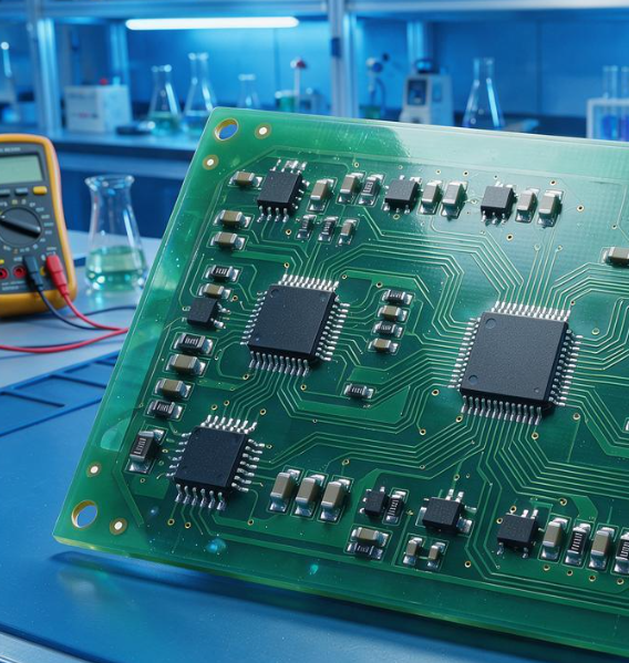
The oxidation resistance of an OSP PCB is often attributed entirely to the PCB manufacturer’s surface-finishing process. However, PCB layout, panelization, packaging, transportation, storage, and assembly conditions can all affect the final performance of an OSP surface finish.
Some PCB designs can create unfavorable manufacturing conditions from the beginning. Even when the OSP chemistry, equipment, and process parameters are well controlled, significant differences in exposed copper distribution or panel flow conditions may make coating uniformity more difficult to maintain.
These problems may not be obvious during prototype production because the production volume is small. Once the design enters mass production, small process variations can be repeated across thousands of boards and become a significant quality issue.
In addition, the OSP film is extremely thin and can be vulnerable to mechanical damage, moisture, contamination, and excessive thermal exposure. Therefore, controlling PCB oxidation requires a complete protection chain covering DFM design, panelization, surface finishing, packaging, storage, and assembly.
1. How Copper Distribution Affects OSP Coating
OSP, or Organic Solderability Preservative, is formed through a chemical reaction between the exposed copper surface and the OSP solution. The distribution and geometry of exposed copper areas can influence solution exchange and process uniformity.
A PCB with large exposed-copper areas in one region and many small isolated pads in another may present different chemical and fluid-flow conditions during processing.
Large exposed copper areas generally provide different solution-contact conditions from isolated fine-pitch pads surrounded by solder mask. Small or densely packed pads may be more sensitive to solution exchange, surface cleanliness, and process uniformity.
BGA arrays deserve particular attention. Pads located in the interior of a dense BGA pattern may have less favorable solution access than pads around the perimeter. This does not mean that every BGA center pad will have insufficient OSP coverage, but the geometry should be considered during PCB DFM review.
When possible, avoid placing critical dense-pad components directly in areas of a panel where manufacturing access may be restricted by the panel outline, tooling, or neighboring structures.
Large exposed copper areas also require attention. A very large copper opening can produce differences in local process conditions between the center and edges of the copper area.
Where electrical requirements permit, large exposed copper regions can sometimes be divided by solder-mask dams. This can create more controlled exposed-copper geometries and reduce the size of individual openings.
Another useful technique is the use of copper balancing features or dummy copper in appropriate non-functional areas. The purpose is to make the overall panel copper distribution more uniform.
However, dummy copper should not automatically be exposed for OSP treatment. Leaving unnecessary copper exposed can increase the active copper area and consume process chemistry without providing an electrical benefit.
2. Panelization and Its Effect on OSP Consistency
Panelization becomes increasingly important during high-volume production.
The position of each PCB within a production panel can influence its exposure to the chemical process, equipment movement, spray or immersion conditions, and other manufacturing variables. Boards near panel edges may experience different process conditions from boards located near the center.
This means that poor can increase variation between individual boards in the same production batch.
A properly designed panel should therefore consider:
- Product distribution across the panel
- Panel edge effects
- Process rails
- Tooling holes
- Clamping locations
- Copper balancing
- Routing and V-Cut structures
- Board-to-board spacing
- Board orientation
A process frame around the product area can provide space for tooling and handling while separating functional PCBs from the immediate panel edge. The exact frame width should be determined with the PCB manufacturer’s equipment and tooling requirements rather than using one universal dimension.
Copper balancing features can also be added to appropriate process areas to help improve panel symmetry and manufacturing consistency.
3. Keep Critical Pads Away From High-Risk Panel Features
V-Cut lines, routed slots, tooling holes, breakaway structures, and panel edges can affect local manufacturing conditions.
Critical BGA pads, fine-pitch components, and other oxidation-sensitive exposed copper areas should be positioned with sufficient clearance from these features.
V-Cut and routed structures can also affect panel rigidity and handling. During manufacturing and depanelization, mechanical movement may cause boards to shift or rub against one another. This can damage a thin OSP film even when the chemical coating itself was initially acceptable.
The panel design should also avoid combining boards with extremely different dimensions or thicknesses without considering the process capability of the manufacturing line.
Mixed panel structures can complicate handling, chemical exposure, thermal behavior, and mechanical support.
Tooling and clamping points are particularly important. Clamping areas should preferably be located on the process frame rather than on functional PCB areas.
Before production, the customer and PCB manufacturer should confirm the tooling and clamping locations during PCB DFM review.
4. Packaging Requirements for OSP PCBs
After surface finishing, packaging becomes the next major protection stage.
An OSP coating creates a very thin organic protective film on exposed copper. Unlike a metallic surface finish, the film does not provide the same level of mechanical protection as a relatively thick metal coating.
Mechanical friction, contamination, excessive moisture, and unsuitable handling can therefore reduce surface quality and increase the risk of PCB oxidation.
Board-to-Board Separation
Individual boards should be separated during packaging to minimize direct contact between exposed pads.
Suitable interleaving materials should be selected based on the customer’s cleanliness and chemical requirements. Low-contamination, sulfur-controlled materials are preferable where sulfur-related surface discoloration is a concern.
Ordinary packaging paper should not be used automatically. The packaging material should be evaluated for chemical compatibility, cleanliness, fiber shedding, and contamination risk.
Moisture-Barrier Packaging
For applications requiring extended storage or high environmental protection, moisture-barrier packaging can be used together with an appropriate desiccant and humidity indicator.
The packaging system should be selected according to the OSP supplier’s process, expected storage period, shipping conditions, and customer requirements.
The objective is to limit moisture ingress rather than simply creating a vacuum. The package should maintain its moisture-barrier performance throughout transportation and storage.
Cool Before Sealing
PCB assemblies or boards that have recently undergone drying or thermal treatment should be allowed to cool to an appropriate temperature before final moisture-barrier packaging.
Sealing a hot PCB can increase the temperature and relative humidity conditions inside the package after cooling, depending on the remaining moisture and package volume.
Proper cooling and controlled packaging help reduce unnecessary moisture exposure to the OSP surface.
Outer Carton Protection
The outer shipping carton should provide sufficient mechanical protection to prevent excessive compression, impact, and movement.
Boards should not be allowed to shift repeatedly inside the package during transportation. Mechanical friction between boards can damage exposed OSP surfaces.
Storage conditions, handling instructions, and recommended use periods should also be clearly communicated to downstream users.
5. Storage and Handling After Packaging
Even well-packaged PCBs can develop oxidation or solderability problems if storage and handling are poorly controlled.
Storage temperature and humidity should follow the OSP supplier’s recommendations and the packaging specification. A controlled, dry environment away from direct sunlight, water sources, condensation, and excessive temperature fluctuations is generally preferred.
A fixed storage period should not be applied universally to every OSP PCB. Shelf life depends on the OSP chemistry, coating quality, packaging system, storage environment, PCB cleanliness, and customer assembly process.
Once moisture-barrier packaging is opened, the exposure clock effectively begins.
Operators should inspect the package and humidity indicator before releasing the boards to SMT production. If the packaging has been compromised or the board has been exposed beyond the supplier’s recommended period, direct assembly should not be assumed to be acceptable.
A solderability evaluation or other appropriate verification can be performed when exposure conditions exceed the established control limits.
For sensitive production programs, storing opened PCBs in a controlled dry cabinet can reduce additional moisture exposure. The appropriate humidity limit should be established according to the material and customer process specification.
6. Reflow Exposure and OSP Surface Protection
OSP is designed to protect exposed copper until soldering, but the protective film is consumed or altered during the soldering process.
Therefore, the number of thermal exposures should be considered during process planning.
It is not technically appropriate to state that every OSP PCB can withstand exactly two complete reflow cycles. The actual limit depends on the specific OSP chemistry, coating thickness and quality, thermal profile, peak temperature, time above liquidus, atmosphere, flux system, and PCB design.
For double-sided SMT assembly, the production sequence should be optimized to minimize unnecessary thermal exposure and storage between reflow operations.
If a board must undergo multiple reflow cycles or repeated rework, solderability validation should be performed using the actual assembly process.
This is particularly important for high-density boards where small changes in surface condition can affect fine-pitch soldering.
7. PCB Specifications Should Define OSP Quality Requirements
Many production specifications simply state “OSP finish required” without defining the associated quality and packaging requirements.
This can create disagreements between customers and PCB manufacturers when oxidation or solderability problems occur.
A more complete specification can include:
- OSP surface-finish type and applicable standard
- Coating thickness or process-control requirements where applicable
- Surface cleanliness requirements
- Solderability acceptance criteria
- Required aging or environmental testing
- Packaging method
- Moisture-barrier requirements
- Interleaving material requirements
- Desiccant and humidity-indicator requirements
- Storage conditions and recommended shelf life
- Open-package exposure requirements
- Reflow and rework limitations
For high-reliability products, these requirements should be included in the purchasing specification or quality agreement rather than communicated informally.
8. OSP PCB DFM Checklist Before Mass Production
A practical PCB DFM review can identify potential OSP risks before production begins.
Layout review
- Check the distribution of exposed copper areas.
- Identify isolated fine-pitch pads and dense BGA regions.
- Review large exposed-copper openings.
- Evaluate whether dummy copper can improve panel copper balance.
- Avoid unnecessary exposed copper that increases chemical loading.
Panelization review
- Confirm process-frame dimensions with the manufacturer.
- Review panel edge effects.
- Confirm tooling and clamping locations.
- Keep critical pads away from V-Cut and routed features.
- Check board spacing and orientation.
- Avoid problematic combinations of significantly different board sizes or thicknesses.
Packaging review
- Define board separation requirements.
- Specify suitable low-contamination interleaving materials.
- Define moisture-barrier packaging requirements where necessary.
- Specify desiccant and humidity-indicator requirements.
- Confirm cooling requirements before sealing.
- Define transportation and storage conditions.
Assembly review
- Confirm the maximum planned thermal exposure.
- Review the actual reflow profile.
- Control the time between unpacking and SMT assembly.
- Establish a solderability verification procedure for extended exposure.
- Minimize unnecessary rework and repeated thermal cycles.
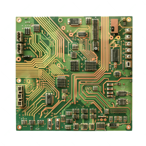
9. Building a Complete OSP Oxidation-Control System
The oxidation resistance of an OSP PCB should not be treated as the responsibility of the surface-finishing department alone.
A reliable control system connects four stages:
Design → Manufacturing → Packaging → Assembly
At the design stage, PCB DFM can reduce unfavorable copper distributions, panel-edge effects, tooling interference, and other structural risks.
During manufacturing, the OSP surface finish chemistry, copper cleanliness, process parameters, coating uniformity, and inspection must be controlled.
After production, PCB packaging should protect the thin OSP film from moisture, contamination, and mechanical damage.
During customer PCB storage and SMT assembly, exposure time, humidity, handling, reflow temperature, and rework conditions must remain within the established process window.
Kingda can integrate OSP requirements into PCB engineering review, panelization, manufacturing, packaging, and production-quality control. By addressing PCB oxidation risks from the beginning of the design process and maintaining control throughout the supply chain, customers can reduce avoidable surface-finish problems and improve consistency during mass production.