PCBA X-Ray Inspection: Hidden Solder Joint Quality Guide
PCBA X-ray inspection is used to see solder joints that are hidden under components. Packages such as BGAs, QFNs, connectors, and components under shields cannot be completely verified by optical inspection because the solder is beneath the body. X-ray technology penetrates the component and displays the internal solder structure, allowing inspectors to find voids, bridges, missing balls, misalignment, and other defects that would otherwise remain invisible until the board fails in the field.
This guide explains how X-ray inspection works, when 2D or 3D imaging should be used, how programs are qualified, and how the technology protects PCBA quality in automotive, medical, industrial, and communications products.
Why X-Ray Is Needed in PCBA
During SMT assembly, many components are placed on top of their solder joints. A BGA connects through small solder balls under the package, while a QFN has exposed pads on its underside. AOI can only inspect surfaces visible to the camera, so a large part of the joint remains unseen.
A hidden defect can create an intermittent connection or a latent reliability risk that is difficult to reproduce during initial test. The board may pass initial testing but fail later under vibration, thermal cycling, or load. X-ray inspection reduces this risk by checking the actual internal connection.
For high-reliability products, X-ray is not optional. Medical, automotive, aerospace, and communication standards often require verification of hidden joints through X-ray or similar non-destructive methods.
Radiation safety is another consideration. X-ray systems must follow local safety regulations, and only trained personnel should operate them. Modern equipment is designed with shielding and interlocks to protect operators during routine use.
How X-Ray Inspection Works
X-ray inspection directs radiation through the PCBA onto a detector. Dense materials such as copper and solder absorb more radiation, creating contrast in the image. The inspector or analysis software can see solder volume, shape, position, and internal voids.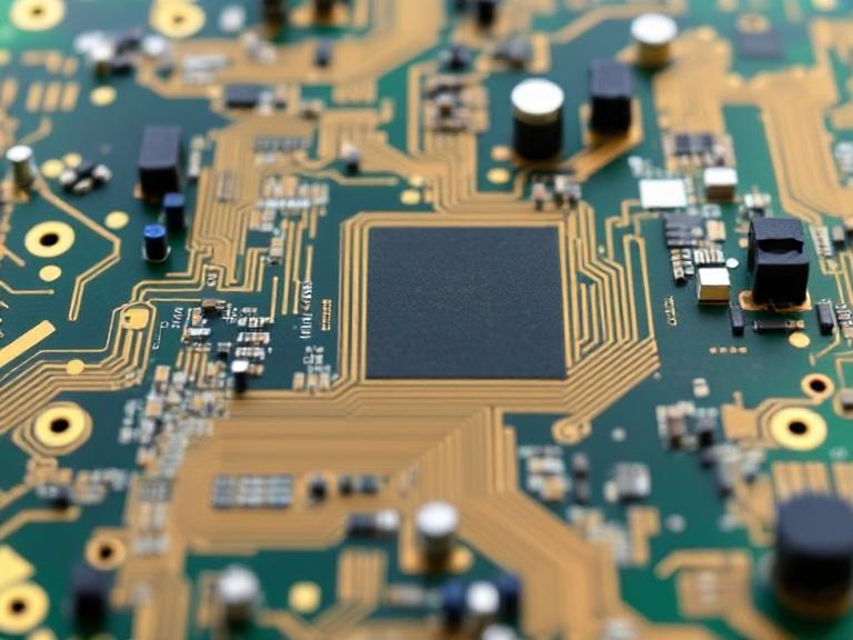
The sample or production board is moved under the X-ray source and detector. Automated systems can inspect multiple boards quickly and compare images to the expected design.
Because the process is non-destructive, the inspected board can continue to assembly or testing without damage.
X-ray equipment must be maintained and calibrated so its images remain reliable. The inspector should also receive training in package construction, solder defect classification, and the limitations of each imaging mode.
2D X-Ray Inspection
2D X-ray is commonly used for through-hole solder inspection, connector pin examination, and general hidden-joint checks. It produces a single projection image of the board and can show solder voids, bridges, and missing material.
2D inspection is faster and usually less expensive than 3D. It is suitable for boards where the critical defect can be seen from one angle and where overlapping features do not hide the joint.
For simple BGA and QFN products, a well-designed 2D X-ray program can provide effective quality control.
3D imaging also helps with components that are mounted on both sides of the board. A 2D image may overlap solder from the top and bottom, making it difficult to judge one joint. The cross-sectional view separates the layers and gives a more reliable result.
3D X-Ray Inspection
3D X-ray or computed tomography takes multiple images from different angles and reconstructs a cross-sectional view of the solder joint. This provides more detailed information about void position, solder height, ball shape, and internal structure.
3D inspection is especially useful for stacked packages, complex modules, and boards where multiple layers of solder overlap in a 2D image. It can distinguish defects that are difficult to confirm with a single projection.
3D X-ray systems cost more and have lower throughput, so the inspection plan should use them where the added information is necessary.
Inspection frequency should also be planned. Some products need 100 percent X-ray coverage, while others can use sampling based on process history and package risk. The plan should be reviewed whenever a new component or process is introduced.
Void Detection and Solder Quality
One of the most important uses of X-ray is void detection. Voids are gas pockets trapped inside the solder joint. A small void may be acceptable, but a large void reduces the conductive area and can crack during thermal cycling.
Acceptance criteria should define the maximum void percentage for each package. The quality engineer compares the X-ray image with the standard and decides whether the board passes.
Void formation can be influenced by solder paste, reflow profile, board finish, and component design. X-ray data helps the process team improve soldering rather than only rejecting bad boards.
When a hidden defect is found, the board should be clearly identified and removed from the normal flow. Rework may be possible for some BGA defects, but the decision should be made with the customer’s acceptance rules in mind because repeated heating can damage the package.
Detecting Bridges and Missing Balls
Solder bridges between BGA balls can create electrical shorts that may not appear at low-current test. X-ray can reveal bridge connections between adjacent balls before they cause a field failure.
Missing or shifted balls are another common BGA defect. The placement machine may pick a component with an incomplete ball array, or the component may shift before reflow. X-ray identifies these problems by showing the complete ball pattern.
Comparing the X-ray image to the design data helps the system detect anomalies automatically.
AXI programs should be validated on known-good and known-bad samples so the defect detection threshold is meaningful. False rejects slow production, while false accepts defeat the purpose of the system.
Automated X-Ray Inspection
Automated X-ray inspection, or AXI, is designed for production lines that need high throughput. Boards move through the system automatically, and software compares each solder joint with the acceptable pattern.
AXI can inspect every board in a lot, which is valuable for high-volume products with hidden joints. It generates defect reports and records images for traceability.
The inspection program should be developed for each board design and updated after changes to the layout, component, or process.
Defect reports should include clear images and a consistent defect code. This allows the quality team to compare trends across production runs and to share understandable data with customers during audits or corrective action reviews.
X-Ray and Process Improvement
X-ray data is not only used to sort good and bad boards. It can show the process team whether void levels are increasing, whether a stencil change affected solder volume, or whether a reflow profile needs adjustment.
When a defect pattern changes, engineers can trace the problem to the related material or equipment and correct it before many boards are affected.
This continuous feedback loop is one of the main benefits of adding X-ray to the PCBA process.
Boards with stacked microvias, module-on-board construction, or components under metal shields may also need X-ray because the internal connections are completely inaccessible to visual methods.
Applications That Require X-Ray
Automotive electronics need X-ray because vehicle systems face vibration, temperature, and long operating life. Medical devices need it because a board failure can affect patient safety. Industrial controls need it when a machine stop causes production loss.
Communications hardware with many BGAs also benefits from X-ray to verify solder integrity at high data rates.
In each case, the inspection plan should be based on the product risk and the ability of other test methods to catch defects.
The inspection sequence should place X-ray before functional test when possible so expensive test fixtures are not wasted on boards with hidden soldering defects. If functional test fails after X-ray, the cause is more likely an electrical or component issue.
Combining X-Ray with Other Testing
X-ray inspection cannot prove that the circuit works. The board still needs electrical test, functional test, and other verification after assembly. X-ray confirms the physical connection; functional test confirms the electrical behavior.
For this reason, X-ray should be part of a complete quality plan that includes solder paste inspection, AOI, X-ray, ICT, FCT, and final visual check. Each method provides a different layer of confidence.
A controlled SMT PCB assembly process with a professional PCBA testing flow will use X-ray where hidden joints exist and functional test where circuit behavior must be proven.
Choosing an X-Ray Inspection Partner
Ask the supplier which X-ray equipment it uses, whether 3D imaging is available, and how inspection acceptance criteria are defined. Review examples of defect reports for BGA products.
The supplier should also explain how it handles rework after X-ray. Removing a BGA to repair a void is expensive and can damage the board, so the process should be designed to minimize the need for rework.
When X-ray inspection is combined with reliable PCB manufacturing and quality management, customers receive consistent protection against hidden solder defects.
Conclusion
PCBA X-ray inspection is essential for boards that contain BGAs, QFNs, and other hidden solder joints. It detects voids, bridges, missing balls, and misalignment that cannot be seen with AOI.
By combining 2D and 3D X-ray capability with automated systems and process data, a PCBA manufacturer can improve quality, reduce rework, and give customers confidence in every assembled board.