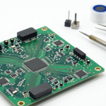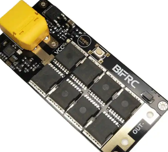
Portable energy storage products rely on a carefully designed 4-layer PCB to integrate battery sensing, BMS protection, inverter control, charging and discharging functions, and power distribution. As the central hardware platform of a portable power system, the PCB must handle high current, switching noise, sensitive measurement signals, thermal stress, and electrical safety requirements within a compact form factor.
A common mistake is to directly adopt a generic industrial-control four-layer stackup without considering the specific characteristics of energy storage systems. High-current power paths, high-impedance sensing circuits, switching nodes, and different voltage domains may coexist on the same board. If the layer structure and return paths are poorly planned, problems such as ground bounce, unstable battery measurements, excessive temperature rise, and electromagnetic interference can appear during prototype testing or certification.
Although a four-layer board has fewer routing resources than a six- or eight-layer board, its layer arrangement has a significant impact on power integrity, signal integrity, thermal behavior, and electrical safety. Selecting the appropriate stackup should therefore be one of the first steps in portable energy storage PCB design.
1. Typical Design Constraints of a Portable Energy Storage PCB
A portable energy storage PCB normally contains two fundamentally different categories of circuits: high-current power circuits and low-level sensing or communication circuits.
Battery-pack voltage sensing and cell-balancing signals generally operate at relatively low current but can be sensitive to switching noise, common-impedance coupling, and ground potential differences. By contrast, the main charging and discharging paths may carry high continuous and transient currents. High-speed switching of MOSFETs can also generate rapid voltage and current transitions that create both conducted and radiated noise.
Thermal management adds another challenge. Portable products usually have compact enclosures and limited airflow. The PCB must therefore provide adequate current-carrying capability while helping transfer heat away from power components.
A four-layer PCB can provide a good balance between performance, cost, weight, and manufacturing complexity. However, the available layers must be allocated carefully because there may not be enough dedicated layers for every individual function.
A typical structure consists of:
- L1: Top layer
- L2: Internal layer
- L3: Internal layer
- L4: Bottom layer
The optimal arrangement depends on power level, signal speed, switching frequency, insulation requirements, mechanical structure, and component placement.
2. Main Four-Layer Stackup Options
Option 1: L1 Signal + L2 GND + L3 Power + L4 Signal
One commonly considered structure is:
L1: Signal / Components
L2: GND Plane
L3: Power Plane
L4: Signal / Components
A relatively continuous ground plane on L2 can provide a stable reference for many L1 signal traces. When the reference plane is kept continuous beneath sensitive signals, the signal return path can remain short and predictable.
This arrangement can be beneficial for battery sensing, control signals, and other circuits that require good noise immunity. The L3 power plane can also provide a low-resistance distribution path for suitable power networks.
However, the power plane should not automatically be treated as a universal high-current conductor. Its actual voltage drop depends on copper thickness, plane geometry, current distribution, neck-down regions, vias, and connection points.
For high-current paths, engineers should evaluate whether additional copper on the outer layers or parallel current paths are required.
This stackup can be a practical choice when signal integrity and a continuous ground reference are important, provided that the power distribution and thermal requirements are addressed separately.
Option 2: L1 Power / Signal + L2 Power + L3 GND + L4 Power / Signal
Another possible arrangement is:
L1: Power + Signal / Components
L2: Power Plane
L3: GND Plane
L4: Power + Signal / Components
This structure allows power components and copper paths to be distributed across both outer layers. It can be useful when high-current routing, component placement, and thermal dissipation require greater use of the top and bottom copper layers.
The internal L2 and L3 planes can also provide dedicated power and ground references.
However, mixed power and signal routing on the outer layers requires careful layout control. Sensitive sensing traces should not cross plane splits or pass close to high-voltage switching nodes. When a signal transitions between layers, its return current must also have an appropriate path.
Poorly controlled transitions can increase loop area and create additional noise coupling.
For this reason, the second structure may provide greater routing flexibility for some higher-power designs, but it places greater demands on PCB stackup planning and layout execution.
3. Why Continuous Ground References Matter
A common four-layer design mistake is to use two signal layers and two poorly defined internal layers without maintaining a sufficiently continuous ground reference.
High-speed switching currents always seek a return path. If the reference plane is continuous and located close to the signal layer, the return current can follow a relatively compact path. If the signal crosses a split, void, or inappropriate plane boundary, the return path may become longer and more inductive.
This can increase electromagnetic coupling and affect EMI/EMC performance.
Sensitive battery-sensing traces should therefore be routed with particular attention to their reference environment. Engineers should avoid routing measurement traces across high-current return paths or directly adjacent to rapidly switching power nodes.
For BMS circuits, stable measurement is often more important than simply achieving low trace resistance. Layout should minimize shared impedance between sensing circuits and high-current switching circuits.
4. Match the Stackup With Material and Copper Thickness
The stackup cannot be selected independently of the PCB material and copper structure.
For many portable energy storage applications, FR-4 materials with an appropriate Tg can provide a practical combination of thermal stability, electrical insulation, availability, and cost. The appropriate Tg should be determined according to operating temperature, thermal cycling requirements, assembly process, and reliability targets rather than using one fixed value for every product.
For applications exposed to higher temperatures or more demanding environmental conditions, higher-Tg laminate may be evaluated.
Copper thickness should also be allocated according to circuit function. For example, the outer layers may use heavier copper for high-current power paths while the inner layers use a standard copper thickness for planes or signals, depending on the required current capacity and manufacturer capabilities.
The actual selection should consider:
- Continuous current
- Peak current
- Trace width
- Plane area
- Allowable temperature rise
- Via capacity
- Thermal dissipation
- Etching capability
- Finished board thickness
- Manufacturing tolerances
Using heavy copper across every layer is not necessarily the best solution. Excessive copper can increase etching difficulty, affect fine-line routing, increase material cost, and create additional lamination considerations.
5. Dielectric Thickness and Electrical Safety
The dielectric structure between PCB layers also requires careful consideration.
Reducing the dielectric thickness between power and ground planes can increase interplane capacitance and may improve high-frequency decoupling characteristics in certain designs. However, dielectric thickness cannot be selected solely according to power integrity considerations.
Portable energy storage products may contain several voltage domains, including battery voltage, switched power rails, and low-voltage control circuits. The PCB must meet the applicable insulation, dielectric withstand, clearance, and creepage requirements.
Engineers should distinguish between creepage and clearance:
- Clearance is the shortest distance through air between conductive parts.
- Creepage is the shortest distance along the surface of an insulating material.
The required values depend on working voltage, transient conditions, pollution degree, insulation system, material properties, and applicable safety standards.
Therefore, reducing dielectric thickness simply to increase plane-to-plane capacitance is not appropriate if it compromises insulation design or manufacturability.
6. Optimize Power and Signal Layer Allocation
A practical four-layer design should allocate layers according to electrical function rather than simply dividing the board into equal routing resources.
High-current power paths should be kept short and wide. Where possible, power distribution can use both outer-layer copper and internal planes to reduce resistance and current density.
Sensitive battery-sensing and communication signals should be physically separated from noisy switching nodes. Their reference planes should remain stable, and layer transitions should provide appropriate return-current paths.
A useful design strategy is to divide the board into functional regions:
- Battery input and high-current power section
- Switching power section
- BMS sensing and protection section
- MCU and communication section
- Inverter or output section
The exact partition depends on the product architecture, but the principle remains the same: high-current switching loops should be kept compact, while sensitive measurement circuits should be isolated from strong noise sources.
7. Validate the Stackup With Simulation and DFM
Once the candidate PCB stackup has been established, simulation can be used to evaluate important electrical and thermal characteristics.
For the power section, engineers can analyze:
- DC voltage drop
- Current density
- Power-plane distribution
- Via current sharing
- Local heating
- High-current bottlenecks
For signal circuits, simulation or field analysis can help evaluate return-current paths, coupling, impedance, and potential discontinuities.
The DFM review should be performed at the same time. The selected stackup must be compatible with the PCB manufacturer’s actual lamination process, available core and prepreg materials, copper thickness combinations, registration capability, and finished-board tolerances.
A technically attractive stackup may not be the best production solution if it requires uncommon materials or falls outside the manufacturer’s stable process window.
8. Prototype Verification and Risk Reduction
During prototype testing, particular attention should be paid to full-load operation and worst-case switching conditions.
Recommended validation areas include:
- Battery sensing accuracy
- BMS protection behavior
- Power-path temperature rise
- MOSFET and switching-node temperature
- DC voltage drop
- EMI/EMC performance
- Insulation resistance
- Dielectric withstand where applicable
- PCB warpage and mechanical stability
If battery-sensing signals show unexpected fluctuations, engineers should not immediately assume that the sensing circuit itself is defective. The investigation should also examine ground-plane continuity, return paths, switching-node proximity, via transitions, and power-ground coupling.
Thermal measurements should similarly focus on localized hotspots rather than relying only on average PCB temperature.
9. Selecting the Right Stackup for Different Power Levels
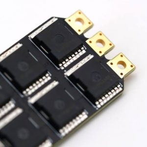
There is no universal four-layer stackup that fits every portable energy storage product.
A lower-power product may prioritize compact routing, cost efficiency, and straightforward manufacturing. A higher-power design may require more extensive copper distribution, stronger thermal paths, more careful switching-loop control, and greater separation between noisy power circuits and sensitive measurement circuits.
Instead of selecting a stackup solely according to nominal wattage, engineers should consider the complete electrical architecture, including battery voltage, continuous and peak current, switching frequency, thermal environment, sensing accuracy, EMI requirements, and applicable safety standards.
This approach produces a more robust PCB stackup than simply copying a standard four-layer template.
Conclusion
For portable energy storage products, four-layer PCB stackup selection is fundamentally an exercise in balancing power distribution, signal integrity, thermal performance, EMI control, electrical safety, and manufacturability.
A well-designed structure can provide continuous reference planes for sensitive signals, efficient copper paths for high-current circuits, and appropriate isolation between noisy switching sections and precision sensing circuits.
The key is to avoid blindly adopting a generic four-layer structure. Instead, the PCB stackup should be developed around the product’s actual power architecture and validated through simulation, DFM review, prototype testing, and reliability evaluation.
Kingda can support portable energy storage projects with PCB stackup design evaluation, DFM analysis, material and copper-thickness selection, prototype fabrication, and volume production. Early collaboration between PCB designers and manufacturing engineers can help establish a stackup that is electrically sound, thermally manageable, safe, and practical for mass production.