PTFE PCB: Low-Loss Laminate for High Frequency RF Boards
A PTFE PCB is built on a polytetrafluoroethylene laminate rather than the usual woven-glass epoxy, and it exists because ordinary FR-4 runs out of performance somewhere above a few gigahertz. The material behaves differently at every stage: how it is drilled, how it is laminated, how the copper is prepared and what it costs. This guide covers what the laminate actually offers, where its limits are, and when paying for it is justified.
What a PTFE PCB Actually Is
A PTFE PCB uses a fluoropolymer dielectric, usually reinforced with a small amount of glass or ceramic filler so that it can be handled as a sheet. The resin is chemically inert, extremely low loss and stable over a wide temperature range, which is why the material appears in radar, satellite and test equipment rather than in consumer products.
It is not a single material. Laminates differ in filler content, glass weave, copper type and thickness, and those choices change the electrical result. Selecting an rf pcb material properly means matching the grade to the frequency band and the mechanical environment of the finished board.
Low Dielectric Constant and Signal Speed
The headline property is a low dielectric constant, typically around 2.1 compared with roughly 4.4 for standard FR-4. Signal propagation slows as the square root of the dielectric constant, so a lower value shortens delay, narrows the effective wavelength on the trace and allows wider features for a given impedance.
That last point is often more valuable than the raw speed. A wider trace at the same impedance carries more current with less conductor loss and tolerates etching variation better. On a high frequency board, the ability to hold 50 ohms with a manufacturable geometry is worth more than a fractional delay improvement.
Loss Tangent and Insertion Loss
The second property is the loss tangent, and for many designs it is the deciding one. A low loss tangent means the dielectric absorbs very little of the field that passes through it, so insertion loss grows slowly with frequency instead of climbing steeply. Above about 10 GHz that difference separates a usable channel from an unusable one.
Loss is not only dielectric. Conductor loss, surface roughness and the skin effect all contribute, and at lower frequencies they may dominate. Modelling the link honestly, rather than assuming the laminate alone solves the problem, is what keeps a high frequency design from being over-specified on material and under-specified everywhere else.
Copper Foil and Surface Finish Choices
Rolled annealed copper is typically used because it is smoother than electrodeposited foil, and smoother copper means less conductor loss at microwave frequencies. The roughness of the copper-resin interface effectively increases the path the current must follow, and at high frequency that penalty becomes visible in the measured loss curve.
Surface finish matters for the same reason. Electroless nickel immersion gold, immersion silver and hard gold are common, while hot air solder levelling is avoided because the thick uneven tin layer distorts a microstrip. A finish that is adequate for a control board can be a measurable defect on an rf pcb material used in a microstrip or stripline structure.
Drilling and Lamination Limits
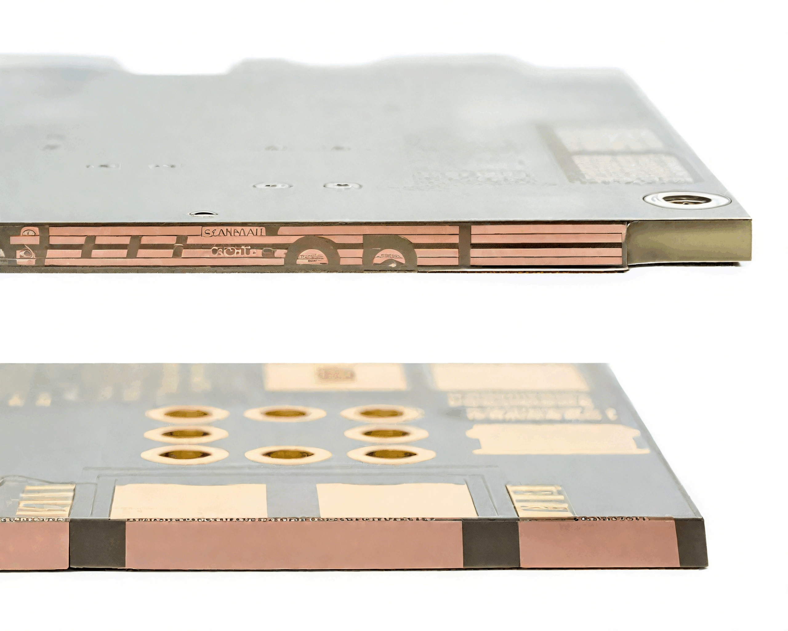
PTFE is soft and has a high coefficient of thermal expansion, so drilling behaves differently than it does in epoxy. Tools blunt faster, hole walls smear rather than cut cleanly, and the drilling parameters have to be reduced. Control of the hole wall is what preserves the plated connection and the impedance of any via in the path.
Multilayer lamination is harder still. The bonding films are specific to the material and the press profile has to be developed for the stackup, so the same dimensions cannot simply be copied from an FR-4 job. A fabricator that builds PTFE regularly will have that profile already; one that does not will learn it at your expense.
Design Rules That Keep the Material Useful
Route with controlled impedance from the start, because the dielectric constant and the substrate height determine the trace width and there is no margin for improvisation later. Keep the ground plane continuous under every high frequency trace, and use stitching vias to tie the reference planes together where the layout forces a change of layer.
Avoid sharp corners and long stubs, both of which create reflections that the low-loss material will faithfully deliver to the receiver rather than absorb. Terminations and connector transitions deserve the same attention, since a mismatch at either end can waste most of the benefit the laminate provides in between.
Cost Drivers and How to Control Them
Cost comes from the laminate itself, from the low panel utilisation of small high frequency jobs, and from the special processing the material requires. Small prototype quantities are priced largely by the sheet area consumed, while volume pricing improves once panels can be shared across a run.
The practical way to control cost is to restrict PTFE to the layers that need it. A hybrid stackup with the antenna or feed layers in fluoropolymer and the digital and power layers in FR-4 keeps most of the electrical benefit while avoiding the price of an all-PTFE construction, and it is far easier for a fabricator to build reliably.
Applications Where the Material Earns Its Place
Antenna feeds, power amplifiers, filters, couplers and phased array elements are the classic uses, because all of them pass a signal through a passive structure that must not add loss. Radar and satellite terminals follow, where the receiver sensitivity is set by the noise figure and every tenth of a decibel in the feed path matters.
Test and measurement hardware is another strong case. Instrumentation has to present a known impedance to the device under test across a wide band, and a fixture built on a laminate that changes its behaviour with frequency undermines the measurement rather than the product. Medical imaging front ends and millimetre wave links round out the list.
Hybrid Stackups and Practical Alternatives
A hybrid stackup bonds fluoropolymer layers to ordinary FR-4 in one press, so the antenna or feed network sits on the low loss material while control, power and digital routing stay on epoxy. The result keeps the critical path quiet and the rest of the board affordable, and it is usually the fastest route to a manufacturable design.
The alternative is to accept higher loss and recover it elsewhere, with a shorter channel, a better receiver or a lower symbol rate. That trade is legitimate, and it should be evaluated with numbers rather than assumed, because a well designed FR-4 board frequently outperforms a poorly specified fluoropolymer one.
Working With a Fabricator on Fluoropolymer
Ask early whether the laminate grade you selected is stocked, because lead times for fluoropolymer sheets are longer than for standard epoxy and a substitute grade changes the impedance calculation. Confirm the copper type as well, since rolled annealed foil is not always the default on a quoted stackup.
Send the stackup drawing with dielectric thickness, copper weight and the target impedance for each controlled layer. If the board is a hybrid, state which layers are fluoropolymer and how the bonding films are arranged, because that detail determines whether the panel can be laminated in a single press.
Related reading: our fabrication notes, board quality and design release notes cover the same ground.
FAQ
Does every high frequency design need PTFE? No. Below a few gigahertz, careful stackup and routing on a good FR-4 can meet the requirement. The laminate becomes necessary when insertion loss or delay variation cannot be met any other way.
Can PTFE boards be assembled like normal boards? They can, but the assembly profile needs attention because the material expands more and conducts heat less readily than epoxy. Reflow profiles are usually adjusted and moisture control before assembly becomes more important.
What drives the price of a PTFE PCB most? The laminate grade and the quantity ordered. Panel utilisation dominates at prototype volumes, so grouping similar boards and standardising the stackup lowers the unit price more than almost any design change.