In electronics manufacturing, development schedules are becoming increasingly demanding. Engineers and product developers often need functional hardware within days rather than weeks to validate a design, identify potential problems, and keep a project on schedule.
This is where Quick-Turn PCB manufacturing becomes especially valuable. A Quick-Turn PCB is manufactured and delivered on an accelerated schedule compared with standard PCB fabrication. It is commonly used for prototype development, urgent engineering changes, design verification, replacement boards, and time-sensitive production requirements.
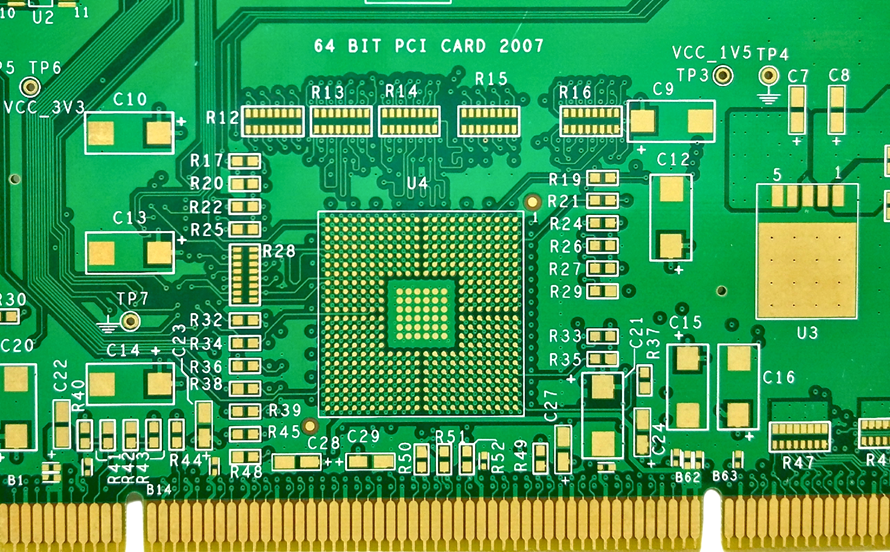
For electronics companies, the value of quick-turn manufacturing is not simply speed. A shorter prototype cycle can help engineering teams identify problems earlier, complete more design iterations, and move products from concept to production faster.
What Is a Quick-Turn PCB?
A Quick-Turn PCB is a printed circuit board manufactured and delivered within a significantly shorter lead time than a standard PCB.
Depending on the board structure, production quantity, materials, and manufacturer’s capacity, standard PCB manufacturing can take days or weeks. Quick-Turn PCB services prioritize the order and streamline engineering, material preparation, fabrication, inspection, and logistics to reduce the overall turnaround time.
Quick-turn PCBs are commonly used for:
- PCB prototypes
- Design verification
- Engineering validation
- Product demonstrations
- Urgent PCB replacements
- Low-volume production
- Production troubleshooting
- Pre-production testing
Importantly, faster production should not mean lower quality. A professional manufacturer should maintain appropriate material specifications, fabrication controls, inspection procedures, and electrical testing while optimizing the production schedule.
Kingda provides rapid PCB and PCBA prototyping as part of its one-stop manufacturing services, supporting projects from PCB fabrication and component sourcing through assembly and testing. Its published information also indicates support for rapid PCBA prototyping, low-volume production, and volume production. (Kingda)
How Quick-Turn PCB Manufacturing Works
Although the schedule is accelerated, Quick-Turn PCB manufacturing still follows the fundamental PCB fabrication process.
Step 1: Design File Review
The process begins when the customer submits manufacturing files such as Gerber or ODB++ data.
The manufacturer reviews the files and checks for potential issues involving:
- Trace width and spacing
- Hole sizes
- Pad dimensions
- Copper clearances
- Solder-mask openings
- Board outline
- Layer configuration
- Manufacturing tolerances
A DFM (Design for Manufacturability) review is particularly valuable for quick-turn orders because manufacturing questions identified after production begins can significantly reduce the time advantage.
Kingda provides DFM/DFA services, Gerber review, BOM verification, component availability analysis, and manufacturing documentation review as part of its engineering support. (Kingda)
Step 2: Material Selection and Preparation
Quick-turn production is easier when commonly used materials are already available.
Standard FR-4, common copper weights, and frequently requested surface finishes can generally be processed more efficiently than highly specialized materials that require additional procurement.
However, material selection should still be based on the electrical, thermal, mechanical, and reliability requirements of the PCB.
Step 3: Inner-Layer Imaging
For multilayer boards, the inner-layer circuit patterns are transferred onto the copper surfaces.
Digital imaging technologies can improve production efficiency and support fine-line PCB fabrication while reducing dependence on traditional phototooling processes.
Step 4: Lamination and Drilling
For multilayer PCBs, individual layers are aligned and laminated under controlled temperature and pressure.
Drilling equipment then creates the required:
- Through-holes
- Vias
- Component holes
- Mechanical openings
The number of layers, hole density, via structure, and required tolerances can significantly affect quick-turn lead time.
Step 5: Copper Plating and Etching
After drilling, copper plating establishes conductive connections through the PCB.
The copper circuitry is then patterned and etched according to the PCB design.
For advanced boards, additional processes may be required for structures such as blind vias, buried vias, microvias, and HDI interconnections.
Step 6: Solder Mask and Surface Finish
A solder mask protects exposed copper and helps reduce solder bridging during assembly.
Depending on project requirements, common surface finishes include:
- HASL
- Lead-Free HASL
- ENIG
- OSP
- Immersion Tin
- Immersion Silver
Standard finishes are generally easier to accommodate within short production schedules than highly specialized finishes.
Step 7: Inspection and Electrical Testing
Before shipment, finished PCBs should undergo appropriate inspection and electrical testing.
Depending on the PCB and customer requirements, this may include:
- AOI
- Electrical continuity testing
- Flying-probe testing
- Visual inspection
- X-ray inspection for applicable structures
Kingda’s published inspection capabilities include SPI, AOI, X-ray inspection, ICT, FCT, and first-article inspection, with inspection methods selected according to product complexity and requirements. (Kingda)
Typical Quick-Turn PCB Lead Times
The actual lead time for a Quick-Turn PCB depends on board complexity, material availability, layer count, quantity, manufacturing tolerances, surface finish, special processes, and shipping.
As a general planning guide:
| Service Tier | Typical Lead Time | Typical Application |
|---|---|---|
| Same-Day / 24-Hour | 1 business day | Simple prototype or urgent replacement |
| 48-Hour | 2 business days | 2–4 layer prototypes |
| 3–5 Day | 3–5 business days | Multilayer prototype boards |
| 5–7 Day | 5–7 business days | More complex multilayer or HDI designs |
These are planning ranges rather than universal guarantees. Customers should confirm whether the quoted lead time includes engineering review, fabrication, assembly, testing, and shipping.
Kingda states that its standard PCB assembly turnaround is generally around 2–3 business days, depending on material availability, design complexity, quantity, surface finish, and other project requirements. It also publishes rapid PCB assembly options for low-volume projects when components are ready. (Kingda)
Benefits of Quick-Turn PCB Services
Faster Time to Market
The most obvious advantage of Quick-Turn PCB services is the ability to shorten the hardware development cycle.
Instead of waiting weeks between prototype revisions, engineers may be able to complete physical testing within days.
This accelerates the workflow:
PCB Design → Prototype → Testing → Revision → Validation → Production
Rapid Prototype Validation
A physical PCB allows engineers to evaluate:
- Electrical performance
- Signal integrity
- Component compatibility
- Mechanical fit
- Thermal behavior
- Connector compatibility
- System-level functionality
This is especially valuable when simulation cannot fully reproduce real-world hardware behavior.
Reduced Development Risk
Identifying a design problem during prototyping is usually less expensive than discovering the same problem after volume production begins.
Rapid prototype cycles make it easier to detect design errors while changes are still relatively inexpensive.
Emergency Production Support
Quick-turn manufacturing can also provide replacement boards when a production problem or unexpected design issue threatens an important schedule.
Faster Design Iteration
Hardware development frequently involves multiple revisions. Shorter PCB fabrication cycles allow engineers to test alternative layouts, components, and circuit architectures without introducing long delays between iterations.
Useful for Low-Volume Production
Quick-Turn PCB manufacturing is particularly useful for:
- Startups
- R&D teams
- Product developers
- Engineering laboratories
- Industrial equipment manufacturers
- Prototype builders
Quick-Turn PCB vs. Standard PCB Fabrication
Quick-turn and standard PCB manufacturing serve different purposes.
| Factor | Quick-Turn PCB | Standard PCB Fabrication |
|---|---|---|
| Lead Time | Often 24 hours to several days | Generally longer |
| Cost Per Unit | Usually higher | Usually lower |
| Production Priority | High | Standard scheduling |
| Material Selection | Often favors stocked materials | Broader options |
| Typical Quantity | Prototype to low volume | Medium to high volume |
| Best For | Prototypes and urgent requirements | Planned production |
| Quality Requirements | Same fundamental requirements | Same fundamental requirements |
The main trade-off is speed versus cost.
Quick-turn production may carry an additional charge because the manufacturer must prioritize the order, reserve production capacity, and potentially use expedited logistics.
For an engineering prototype holding up a larger development program, the premium may be worthwhile. For predictable high-volume production, standard manufacturing is generally more economical.
Applications of Quick-Turn PCBs
Electronics Prototyping
PCB prototyping is the most common application for quick-turn manufacturing.
Startups, OEMs, engineers, and R&D teams can convert PCB design files into physical hardware quickly and use the boards for functional validation.
Aerospace and Defense
Aerospace and defense projects can have demanding schedules for avionics, communication equipment, radar, control systems, and other specialized electronics.
Quick-turn fabrication can accelerate early development while maintaining the required quality and documentation controls.
Automotive Electronics
Modern vehicles use sophisticated electronics for:
- ADAS
- ECUs
- Sensors
- Infotainment
- Battery management
- Vehicle networking
Fast prototype PCB fabrication can shorten hardware validation cycles before products proceed to later development and qualification stages.
Medical Electronics
Medical equipment development frequently requires repeated engineering iterations before formal validation.
Quick-turn PCB services can shorten prototype cycles, although applicable medical quality, traceability, documentation, and regulatory requirements still need to be maintained.
Consumer Electronics
Wearables, IoT products, smart-home devices, and other consumer electronics often undergo several prototype revisions.
Rapid PCB production allows product teams to test physical designs sooner and move more quickly toward final production.
Industrial and Test Equipment
Industrial companies may need custom controller boards, communication interfaces, test fixtures, or replacement boards to reduce equipment downtime.
Quick-turn manufacturing can help shorten troubleshooting and equipment-recovery cycles.
Design Considerations for Quick-Turn PCBs
The PCB design itself can strongly influence whether an accelerated manufacturing schedule is practical.
Use Standard Materials Where Possible
When the application allows, standard materials such as FR-4 and commonly used copper weights are often easier to source quickly.
Specialized high-frequency, high-temperature, or other advanced materials may require additional procurement time.
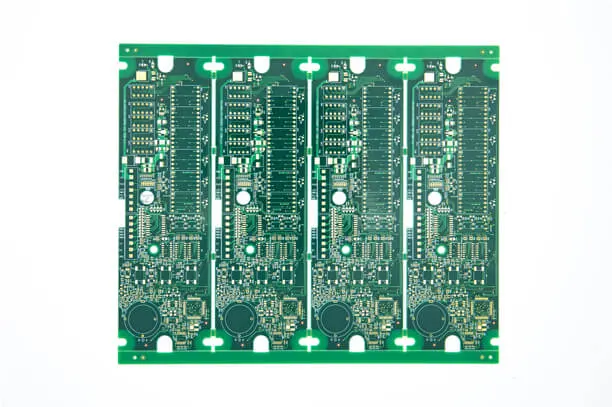
Keep the Layer Count Practical
Two-layer and four-layer PCBs are generally easier to accelerate than complex multilayer constructions.
However, engineers should never reduce layer count solely for speed if doing so compromises signal integrity, power integrity, thermal performance, or manufacturability.
Avoid Unnecessary Tight Tolerances
Extremely small trace widths, fine spaces, microvias, blind/buried vias, controlled impedance, and other advanced structures can increase manufacturing complexity.
Where these features are not required, using standard design rules can improve both cost and turnaround time.
Submit Complete Manufacturing Files
Before submitting an urgent PCB order, verify:
- Gerber files
- Drill files
- Board outline
- Copper layers
- Solder mask
- Silkscreen
- Stackup requirements
- Fabrication notes
Incomplete or inconsistent manufacturing data is one of the simplest ways to lose the time saved by quick-turn fabrication.
Confirm the Stackup Early
For controlled-impedance PCB designs, communicate the required stackup to the manufacturer before production.
Last-minute changes to dielectric thickness, copper thickness, or layer assignment can create additional engineering work and delay production.
Cost Factors in Quick-Turn PCB Manufacturing
The cost of a Quick-Turn PCB depends on both the board itself and the manufacturing priority.
Lead Time
The shorter the requested turnaround, the greater the potential premium.
A one-day order normally costs more than a three- to five-day order for the same board.
Layer Count
Additional layers increase:
- Material consumption
- Lamination cycles
- Drilling requirements
- Processing time
- Inspection requirements
Board Size and Quantity
Larger boards consume more panel area. Increasing production quantity can distribute setup and processing costs across more units.
Surface Finish
HASL is generally economical, while ENIG typically costs more but offers a flatter surface and is commonly selected for fine-pitch applications.
Special Features
Features such as:
- Controlled impedance
- Heavy copper
- Edge plating
- Countersinks
- Blind and buried vias
- Microvias
- Special surface finishes
can increase cost and lead time.
Shipping
For a very fast PCB order, express shipping can become a meaningful part of the total project cost. When comparing suppliers, consider fabrication time + assembly time + shipping time, rather than fabrication time alone.
When Should You Choose a Quick-Turn PCB?
A Quick-Turn PCB service is most valuable when schedule pressure justifies the additional manufacturing cost.
Consider quick-turn manufacturing when:
You Are in Active Prototype Development
Frequent design iterations can make long standard lead times inefficient.
You Have a Fixed Product Deadline
Trade shows, customer demonstrations, internal validation milestones, and launch schedules can create situations where delivery dates cannot easily move.
You Need Urgent Replacement Hardware
A replacement PCB may be required to keep equipment, testing, or production running.
Your Design Is Still Evolving
When the design has not been fully validated, quick-turn prototypes can help avoid committing too early to a large production order.
You Need Functional Hardware Quickly
Physical testing often reveals issues that are difficult to detect through simulation alone.
How Kingda Supports Quick-Turn PCB and PCBA Projects
For companies that need both speed and manufacturing support, choosing a supplier with integrated PCB fabrication and PCBA capabilities can simplify the entire process.
Kingda provides a one-stop manufacturing workflow covering PCB design support, PCB fabrication, component sourcing, SMT assembly, DIP/THT assembly, testing, and final product integration. (Kingda)
Rapid Prototyping and Production Flexibility
Kingda supports rapid PCBA prototyping, low-volume production, and high-volume manufacturing, allowing customers to use the same manufacturing partner as their projects move from engineering validation to production. (Kingda)
DFM/DFA Engineering Support
Kingda’s engineering services include DFM review, DFA analysis, Gerber review, BOM verification, pick-and-place file verification, component availability analysis, and production optimization. These services can help identify manufacturability issues before production and reduce unnecessary prototype iterations. (Kingda)
PCB and PCBA Under One Workflow
Kingda supports a broad range of PCB and assembly technologies, including rigid, flexible, rigid-flex, multilayer, HDI, heavy copper, metal-core, high-TG, high-frequency, and controlled-impedance PCB assemblies. (Kingda)
Inspection and Testing
Kingda integrates SPI, AOI, X-ray, FAI, ICT, and functional testing into its quality-control process according to product requirements. (Kingda)
Quality Management and Traceability
Kingda states that it operates under IATF 16949, ISO 13485, and ISO 9001 quality management certifications, and its published manufacturing process emphasizes production traceability from incoming materials through final shipment. (Kingda)
Component Sourcing
Kingda provides component procurement and supply-chain support, helping customers coordinate PCB assembly projects without managing separate PCB, component, and assembly suppliers. (Kingda)
Cost and Schedule Optimization
The most effective quick-turn strategy is not necessarily to select the fastest possible production option. Kingda’s engineering team can evaluate the PCB design, material availability, quantity, assembly requirements, and testing needs to determine a practical manufacturing approach. This can help customers avoid paying for unnecessary acceleration while still meeting project deadlines. (Kingda)
How to Reduce Quick-Turn PCB Costs
A quick-turn PCB does not have to be unnecessarily expensive. Cost can often be controlled by:
- Using standard PCB materials where appropriate
- Minimizing unnecessary layer count
- Avoiding specialized features unless required
- Using standard surface finishes
- Completing DFM before submitting the order
- Providing clean and complete manufacturing files
- Ordering multiple prototypes together when practical
- Comparing fabrication and shipping costs together
- Selecting the fastest lead time that the project actually requires
For customers who also need assembly, combining quick-turn PCB fabrication with PCB assembly through one supplier can further simplify logistics.
Conclusion
Quick-Turn PCB manufacturing is an important tool for hardware development when time is a critical factor. By shortening the period between PCB design and functional hardware, it helps engineering teams validate designs faster, identify problems earlier, and accelerate product development.
The main advantage of quick-turn manufacturing is not simply shorter fabrication time. Its real value lies in reducing the time between design iterations, allowing teams to test, refine, and validate products more efficiently.
However, speed should not come at the expense of quality. A reliable quick-turn PCB manufacturer should maintain proper materials, fabrication processes, inspection, electrical testing, and traceability while optimizing production scheduling.
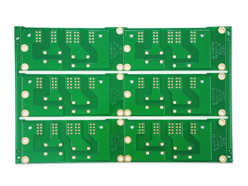
For customers seeking a supplier that can combine quick-turn PCB fabrication, rapid PCBA prototyping, component sourcing, SMT/THT assembly, engineering support, inspection, and testing, Kingda provides an integrated manufacturing solution designed to support projects from prototype through production. (Kingda)