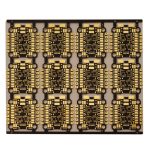
Radar PCB Manufacturing for High-Frequency Use
Radar boards carry signals where small physical changes become large electrical effects. A trace width shift, a dielectric thickness variation, or a rough copper surface can disturb impedance and raise loss. Buyers and engineers therefore need to judge a radar PCB manufacturer on process control, not on price alone. This guide covers the material, stackup, routing, and inspection decisions that decide whether a high-frequency board behaves as designed. It also lists what to verify before you release a lot to production.
Radar systems appear in automotive sensing, industrial measurement, weather monitoring, security, and aerospace platforms. Each use sets its own frequency range, thermal load, and reliability target. The board must carry RF transmission lines, receiver circuits, antenna interfaces, digital processing, and power management together. That mix makes the PCB a system-level component rather than a simple carrier. A supplier who understands this relationship can flag risks early and keep the build repeatable across orders.
What a Radar PCB Does
A radar board transmits electromagnetic energy toward a target and receives the reflected portion. The electronics then process the return to extract distance, direction, or movement. Unlike a low-frequency board, the radar PCB must hold predictable electrical behavior across its whole operating band. Dielectric constant, dissipation factor, copper thickness, and via structure all influence that behavior. Small deviations that would be harmless elsewhere can shift insertion loss or phase on a radar channel.
A typical board combines several functions on one substrate. It may host the RF front end, the antenna feed network, analog conditioning, data conversion, a processor, and power regulation. Each block has different needs for grounding, shielding, and thermal relief. The stackup must separate them without breaking the reference planes that RF traces depend on. Good PCB design and layout work settles these conflicts before fabrication starts, when changes are still cheap.
Material Selection Matters
Laminate choice drives loss, phase stability, and cost more than any other single decision. Standard FR-4 can serve lower microwave bands in some designs, but its losses rise with frequency. PTFE-based laminates and filled hydrocarbon materials offer lower dissipation and steadier dielectric constant. Hybrid builds place high-frequency material only where the RF path needs it and use FR-4 elsewhere. That approach controls cost while keeping critical lines on suitable dielectric.
Engineers should match the material to the actual frequency band, not to a habit. Check dissipation factor, dielectric constant tolerance, thermal conductivity, and moisture absorption against the operating environment. Confirm that the fabricator holds the laminate in stock or has a qualified source. Ask how the supplier handles material traceability, because a quiet laminate change can shift impedance on a finished lot. These questions belong in the quotation stage, before tooling is committed.
Stackup and Impedance Control
The stackup fixes trace geometry, dielectric spacing, and reference plane placement. It should be finalized before routing begins, since later edits often force a rebuild. RF layers need a continuous reference plane directly beneath the signal layer. Power and digital sections should sit away from sensitive receive paths. Symmetry helps control warp during lamination, especially on multilayer RF boards with mixed materials.
Controlled impedance ties the design to the process. The fabricator must know the target impedance, the tolerance window, and which lines are critical. Trace width, copper thickness, and dielectric height are then tuned together during CAM review. A supplier who only etches the supplied files cannot close this loop. Ask for the calculated stackup and the test coupon plan before you approve the order. This is the point where a capable partner earns its value.
Hybrid stackups add a specific failure mode that buyers should understand. When PTFE and FR-4 are laminated together, the two materials expand at different rates under heat. That mismatch can cause delamination at the interface, resin starvation near the bond, or a shift in dielectric height after cure. A fabricator who has run hybrid builds will adjust the lamination cycle and the prepreg choice for the pair. Ask for the bond interface detail and the cure profile before release.

RF Routing and Grounding
Keep high-frequency traces short and direct. Every bend, stub, and via adds a discontinuity that reflects energy. Where a via is unavoidable, place ground vias nearby to give the return current a short path. Avoid routing RF lines across plane splits, because the return current will detour and radiate. Sensitive receive traces deserve extra spacing from digital clocks and switching regulators.
Grounding decides much of the board’s noise behavior. A solid ground plane under the RF section supports clean return currents. Stitching vias tie surface ground to inner layers and reduce cavity resonance. Keep digital return currents out of the RF ground region where possible. Designers should also plan shielding cans and fence vias early, since these features affect the layout and the assembly sequence.
Antenna transitions deserve their own review. The launch from a microstrip or stripline to the antenna feed often creates a small impedance step that is invisible on a schematic. A poorly matched launch raises return loss and wastes transmit power. Designers should model the transition, keep the ground reference continuous through it, and check the pad geometry against the connector footprint. Buyers can ask whether the fabricator has built similar launches and what coupon data confirmed them.
Fabrication Process Control
High-frequency boards demand tight control at every step. Inner-layer imaging and etching must hold trace width within the agreed window. Lamination needs a profile matched to the laminate system, because PTFE and hydrocarbon materials behave differently under heat and pressure. Drilling parameters affect via wall quality and impedance. Plating thickness must meet the target without closing small features.
Each step feeds the next, so a single drift can spoil a lot. Registration errors on multilayer RF boards shift impedance and can short inner layers. Resin smear or poor hole cleaning weakens plated connections. Surface finish choice also matters, since some finishes suit fine-pitch RF pads better than others. A factory with written process sheets and recorded parameters can trace a defect to its cause. That traceability is what separates a controlled build from a hopeful one.
Etch compensation is a quiet variable that buyers rarely see. The etcher removes copper laterally as well as vertically, so a trace drawn at a given width will finish narrower. For a 50-ohm line on thin dielectric, that loss of width raises impedance. A capable fabricator applies etch compensation per layer and per copper weight, then verifies the result on the coupon. Ask whether the process sheet lists the compensation factor and how often it is rechecked against measured traces.
Inspection and Test Coverage
Inspection catches defects before shipment, but its greater value is feedback. When a joint or trace fails, the engineer learns whether imaging, lamination, or drilling caused it. That closed loop pushes defect rates down over time. Visual checks alone are not enough for radar boards. Electrical verification, impedance coupon measurement, and functional test each add confidence in the finished product.

Ask what the supplier measures and what it records. A serious program includes automated optical inspection, X-ray for hidden joints, dimensional checks, and electrical test on every board. Coupon data should confirm that impedance landed inside the window. A structured quality management system keeps these records with the lot, so a field return can be traced quickly. Buyers should request the test report as a routine part of each order.
Coupon design itself deserves a question. A test coupon only proves the process if its geometry matches the production traces. If the coupon uses a wider line or a different dielectric build, the measured impedance says little about the board. Ask the fabricator to place coupons on the same panel, built with the same stackup and the same etch step. Confirm how many coupon sites are measured per lot and what happens when a reading falls outside the window.
Prototype to Production Path
Radar projects rarely reach volume in one step. Early samples reveal pad geometry issues, component tolerances, and process behavior before thousands of boards are committed. Treat the pilot run as part of the project, not as an extra cost. Validate RF performance, impedance, antenna interface, thermal behavior, and mechanical fit on the first articles. Fix what the data shows, then release the design for volume.
Moving from prototype to production should keep the same process settings and material sources. A supplier who can run both stages under one roof reduces the risk of a silent change. For teams that need assembled units, rapid PCBA prototyping shortens the loop between design and a working sample. Later, high-volume PCB assembly carries the validated build into steady output. Component procurement then decides whether the supply chain supports that schedule.
Watch for silent changes when a design moves to volume. A fabricator may switch to a different prepreg lot, a new laminate supplier, or a faster drill recipe to meet a delivery date. Any of these can shift impedance or via quality without a design change. Buyers should require written notice before any material or process substitution and should recheck the first production lot against the prototype coupon data. That single habit catches most of the drift that appears after a successful pilot.
Choosing the Right Partner
Compare suppliers on capability, not on headline price. Ask about high-frequency experience, laminate availability, impedance control, and multilayer or HDI capacity. Check how the factory reviews files before production and whether it raises engineering questions early. Confirm the inspection equipment and the records kept with each lot. A partner who recommends a manufacturable structure is worth more than one who simply accepts the files.
Finally, confirm the practical details. Can the supplier hold the tolerance the product needs without charging for accuracy nothing uses? Does it keep material certificates and process data for repeat orders? Will it support both prototype and production quantities without changing the build? The answers decide the real cost of the board. A radar PCB that meets its electrical targets on the first lot and every lot after is the outcome worth buying.