Amplifier PCB Manufacturer
High-performance amplifier circuits require a PCB that can manage signal integrity, power distribution, thermal conditions, and electromagnetic interference. A properly engineered Amplifier PCB provides a stable platform for signal amplification while supporting the electrical and mechanical requirements of the final product.
Modern amplifier applications range from consumer audio equipment and professional sound systems to automotive electronics, industrial control equipment, medical devices, and wireless communication systems. Depending on the application, the PCB may require multilayer construction, controlled impedance, high-Tg materials, high-frequency laminates, heavy copper, or hybrid material structures.
For projects requiring customized board structures, material selection, and manufacturing support, professional PCB Manufacturing services can help ensure that the finished board meets both electrical and production requirements.
What Is an Amplifier PCB?
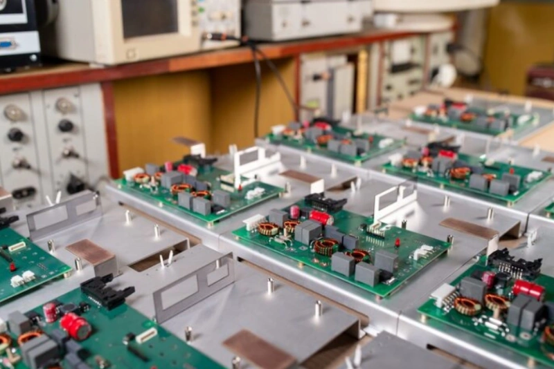
An Amplifier PCB is a printed circuit board specifically designed to support an electronic amplifier circuit. Its primary function is to provide electrical connections between amplifier ICs, transistors, resistors, capacitors, connectors, power circuits, and other components while maintaining the required signal and power characteristics.
Amplifier PCBs are widely used in audio systems, communication equipment, industrial electronics, automotive systems, medical equipment, and other electronic products that require signal amplification.
The PCB design has a direct influence on amplifier performance. Trace routing, grounding, component placement, power delivery, thermal management, and PCB material selection must all be considered during development.
For more complex amplifier products, engineers may combine PCB fabrication with PCB Design and Layout support to optimize the board before production.
Key Features of Amplifier PCB Manufacturing
A professionally manufactured amplifier circuit board may require several specialized technologies and materials depending on the operating frequency, power level, and application environment.
Advanced PCB Materials
Common material options include standard FR-4, high-Tg FR-4, high-speed and low-loss laminates, PTFE-based materials, ceramic-filled materials, and hybrid constructions.
For high-frequency amplifier circuits, low dielectric constant and low dissipation factor materials can help maintain signal integrity and reduce transmission losses.
Controlled Impedance
High-frequency amplifier circuits may require controlled impedance to maintain predictable signal transmission. Accurate stack-up design, trace geometry, dielectric thickness, and material selection are important factors in achieving the required impedance.
Advanced Via Structures
Depending on circuit density, amplifier boards may use plated through holes, blind vias, buried vias, microvias, staggered vias, or stacked via structures.
These technologies can help optimize routing space and support compact, high-density circuit designs.
Thermal Management
Power amplifiers can generate significant heat during operation. PCB construction must therefore consider copper thickness, thermal vias, component placement, heat spreading, and the interface between the PCB and external heat dissipation structures.
For high-power applications, Heavy Copper PCB technology may be considered when increased current-carrying capacity and improved thermal performance are required.
Surface Mount and Through-Hole Components
Amplifier PCBs may use SMT components, through-hole components, or a combination of both technologies. The choice depends on electrical performance, mechanical strength, component availability, assembly requirements, and the intended application.
For mixed component configurations, Mixed Technology PCB Assembly combines surface-mount and through-hole assembly processes within the same production solution.
Advantages of Amplifier Circuit Boards
Compact and Efficient Design
PCB technology allows amplifier components to be arranged in a compact and repeatable structure. Careful component placement can shorten signal paths, simplify power distribution, and reduce unnecessary parasitic effects.
Reliable Electrical Performance
A properly designed Amplifier Circuit Board provides stable electrical connections and consistent signal transmission. Appropriate grounding, power distribution, and routing practices can help reduce noise and unwanted interference.
Improved Signal Integrity
Signal integrity is particularly important for audio, RF, and high-speed amplifier applications. Controlled routing, appropriate stack-up structures, suitable materials, and effective grounding can help reduce signal degradation.
Scalable Production
Amplifier PCBs can be produced for prototypes, small production runs, or larger commercial programs. This allows manufacturers to support product development from initial engineering validation through volume production.
For development-stage products, Prototype PCB Assembly can accelerate the transition from PCB design to functional testing.
Cost-Effective Manufacturing
Optimized PCB layouts can reduce material consumption, simplify assembly, improve production yield, and minimize unnecessary manufacturing complexity. Early engineering review can also identify potential production problems before fabrication begins.
Easier Maintenance and Troubleshooting
A well-organized PCB makes it easier to identify components, test electrical nodes, trace signals, and diagnose faults during development and servicing.
Applications of Amplifier PCB
Home Audio and Entertainment Systems
Amplifier boards are widely used in home audio systems, soundbars, AV equipment, home theater systems, active speakers, and other consumer electronics.
Audio amplifier designs must balance output power, noise performance, thermal behavior, and signal quality.
Professional Audio Equipment
Professional amplifiers used in recording studios, concert systems, broadcast equipment, and commercial sound systems often require higher power levels and reliable long-term operation.
These applications can require carefully designed power sections, robust grounding, thermal management, and high-quality components.
Portable Audio Devices
Bluetooth speakers, headphones, portable speakers, and battery-powered audio products require compact amplifier circuits with efficient power consumption.
Small board dimensions and high component density make PCB layout particularly important for these products.
Industrial Electronics
Industrial equipment may use amplifier circuits for sensors, control systems, measurement equipment, communication systems, monitoring devices, and automation equipment.
Industrial applications generally require reliable operation under demanding environmental and electrical conditions. Industrial PCB Assembly can support products requiring customized PCB structures and production volumes.
Medical Electronics
Amplifier circuits are found in various medical and diagnostic electronics where weak signals must be detected, conditioned, or amplified.
These applications require careful consideration of electrical noise, reliability, manufacturing consistency, and applicable quality requirements.
Automotive Electronics
Automotive audio systems, communication modules, sensor interfaces, and other electronic systems may incorporate amplifier circuits.
Automotive PCB applications can require enhanced thermal performance, vibration resistance, reliability, and controlled manufacturing processes.
Why Amplifier PCB Design Matters
The PCB layout has a direct influence on amplifier performance. Even when the circuit schematic is correct, poor PCB implementation can introduce unwanted noise, signal degradation, thermal problems, and electromagnetic interference.
Important design considerations include:
- Signal path optimization: Keep sensitive signal paths short and avoid unnecessary routing.
- Grounding: Use an appropriate grounding strategy to minimize noise and unwanted ground-loop effects.
- Power distribution: Ensure that power traces and planes can safely carry the required current.
- Component placement: Position critical components according to the electrical characteristics of the circuit.
- Thermal management: Keep high-power components away from temperature-sensitive devices where practical.
- EMI control: Separate sensitive analog signals from noisy switching and high-current sections.
- Manufacturability: Design within the manufacturer’s validated production capabilities.
For complex boards, engineering review and DFM analysis can identify potential manufacturing risks before fabrication.
Amplifier PCB Layout and Design Considerations
Select the Appropriate Layer Stack-Up
Many amplifier boards use two-layer or four-layer construction, while more complex products may require six or more layers.
A typical four-layer structure may include signal and component routing on the outer layers with dedicated ground and power structures in the inner layers. The final stack-up should be selected according to circuit complexity, current requirements, impedance requirements, thermal conditions, and available space.
Optimize Decoupling Capacitors
Decoupling capacitors should generally be positioned close to the relevant IC power pins. Short connections between the capacitor and power/ground pins help reduce unwanted inductance and improve local power stability.
Separate High-Power and Sensitive Signals
High-current power paths and switching nodes can generate electrical noise. Sensitive analog or audio signals should therefore be routed away from noisy power sections whenever possible.
Use Appropriate Trace Widths
Trace width must be selected according to current, copper thickness, temperature rise, and applicable design requirements.
High-power amplifier outputs may require significantly wider copper traces than low-current signal lines.
Control Parasitic Effects
Parasitic capacitance and inductance can influence amplifier stability and high-frequency performance. Excessive routing length, large loops, poorly positioned vias, and inappropriate component placement can increase unwanted parasitic effects.
Consider Thermal Design Early
Thermal design should not be treated as an afterthought. Copper areas, thermal vias, component spacing, heat sinks, airflow, and enclosure design should be considered together during the PCB development process.
Materials for Amplifier PCB
The appropriate PCB material depends on operating frequency, power level, thermal requirements, signal integrity, cost, and environmental conditions.
Standard FR-4
FR-4 is suitable for many conventional audio, industrial, and consumer amplifier applications where extreme high-frequency performance is not required.
High-Tg FR-4
High-Tg materials provide improved thermal resistance and can be useful for amplifier applications that experience elevated operating temperatures.
High-Frequency Materials
Low-loss materials are suitable for RF and high-frequency amplifier designs where dielectric performance and signal transmission characteristics are critical.
PTFE and Hybrid Materials
PTFE-based laminates and hybrid PCB structures can be used for demanding high-frequency applications. Material selection should be based on the operating frequency and required electrical characteristics rather than simply choosing the most advanced material.
Heavy Copper
Heavy copper construction can be beneficial for high-current amplifier designs by increasing current-carrying capacity and improving heat distribution.
Amplifier PCB Manufacturing Process
A reliable Custom Amplifier PCB typically follows a controlled manufacturing workflow:
- Engineering and design review
- Gerber and manufacturing file verification
- Material and stack-up selection
- PCB fabrication
- Surface finishing
- Electrical testing
- Component procurement when assembly is required
- SMT and/or through-hole assembly
- AOI and X-ray inspection where applicable
- Functional and electrical testing
- Final inspection
- Packaging and shipment
Integrating PCB fabrication and assembly under one manufacturing workflow can reduce communication problems and simplify production management. Turnkey PCB Assembly can combine PCB fabrication, component procurement, assembly, inspection, and related manufacturing services.
Quality Control for Amplifier PCB
Quality control is essential because amplifier boards can be sensitive to electrical noise, component variation, thermal stress, and manufacturing defects.
Depending on the project, quality procedures may include:
- Incoming material inspection
- PCB dimensional inspection
- Automated optical inspection
- X-ray inspection for applicable components
- Electrical testing
- Solder joint inspection
- Functional testing
- Component verification
- Final visual inspection
- Manufacturing traceability
For production assemblies, PCBA Testing and Quality Inspection can help verify assembly quality and electrical performance before shipment.
How to Choose an Amplifier PCB Manufacturer
When selecting an Amplifier PCB Manufacturer, consider more than the quoted PCB price. The manufacturer should have the technical capabilities required for the project’s material, layer count, impedance, thermal, assembly, and testing requirements.
Important evaluation criteria include:
- PCB fabrication capabilities
- High-frequency and controlled-impedance experience
- Multilayer manufacturing capability
- Material availability
- SMT and through-hole assembly capability
- Component sourcing capability
- DFM/DFA engineering support
- Electrical and functional testing
- Quality management systems
- Prototype-to-production support
- Production scalability
- Delivery capability
A manufacturer capable of handling both PCB fabrication and assembly can provide a more streamlined supply chain for complex amplifier products.
Why Choose GOPCBA for Amplifier PCB Manufacturing?
GOPCBA provides integrated PCB and PCBA manufacturing services covering PCB design, fabrication, component procurement, SMT assembly, through-hole assembly, testing, and final product integration.
The company supports PCB projects ranging from prototypes and low-volume production to larger manufacturing programs. Its published capabilities include multilayer, HDI, high-frequency, high-TG, heavy-copper, flexible, rigid-flex, and controlled-impedance PCB technologies.
For amplifier applications, this integrated manufacturing approach can simplify engineering communication, material sourcing, fabrication, assembly, inspection, and production management.
Get a Quote for Your Amplifier PCB Project
Whether you are developing a compact audio amplifier, industrial signal amplifier, automotive electronics module, or high-frequency amplification system, the PCB should be engineered around the actual electrical, thermal, mechanical, and manufacturing requirements of the product.
Provide your Gerber files, PCB specifications, BOM, drawings, layer requirements, material preferences, and production quantity for an engineering review and quotation.
GOPCBA can support the process from PCB fabrication and assembly through testing and production, helping turn your amplifier PCB design into a reliable manufactured product.
Frequently Asked Questions
What is an amplifier PCB?
An amplifier PCB is a printed circuit board designed to electrically and mechanically support an amplifier circuit, including its signal, power, control, and protection components.
What is the main purpose of an amplifier PCB?
Its main purpose is to provide reliable electrical interconnections and an optimized physical platform for amplifying audio, RF, sensor, communication, or other electronic signals.
What types of amplifier PCBs are available?
Amplifier PCBs can be single-sided, double-sided, or multilayer boards. Depending on the application, they may also use rigid, flexible, rigid-flex, high-frequency, high-Tg, heavy-copper, or controlled-impedance constructions.
What materials are commonly used for amplifier PCBs?
FR-4 is common for conventional applications, while high-Tg, low-loss, PTFE-based, ceramic-filled, and hybrid materials may be selected for higher-frequency or higher-temperature applications.
How many layers does an amplifier PCB need?
The layer count depends on circuit complexity, routing density, power requirements, impedance control, grounding strategy, and thermal considerations. Two- and four-layer boards are common, while more complex applications may require six or more layers.
How can amplifier PCB performance be improved?
Performance can be improved through optimized component placement, short signal paths, proper grounding, appropriate power distribution, controlled impedance, effective decoupling, thermal management, and careful EMI control.
What is the difference between an ordinary PCB and an amplifier PCB?
An amplifier PCB is specifically optimized for signal amplification. It may require greater attention to grounding, signal integrity, power distribution, thermal management, noise reduction, and component placement than a general-purpose circuit board.
Can amplifier PCBs be manufactured in low volumes?
Yes. Prototype and low-volume production are suitable for product development, engineering validation, testing, and early market launches. Low Volume PCB Assembly can help manufacturers move from prototype quantities toward production more efficiently.
What information is needed for an amplifier PCB quotation?
Typical quotation documents include Gerber files, PCB specifications, layer count, material requirements, stack-up information, surface finish, PCB quantity, BOM, pick-and-place files, assembly drawings, and testing requirements.
How can I start an amplifier PCB project?
Prepare your PCB design files and technical requirements, then submit them to GOPCBA for engineering review and quotation. The manufacturing team can evaluate PCB fabrication, component assembly, testing, and production requirements before starting the project.