radar system PCB High-Frequency Manufacturing Requirements and Reliability
Why High-Frequency PCBs Matter in Radar Systems
Radar systems rely on high-frequency electromagnetic signals to detect, locate, track, and identify targets. Within these systems, the PCB provides the electrical platform for RF signal transmission, processing, control, and power distribution.
As operating frequencies continue to increase, PCB performance becomes increasingly important. Signal loss, impedance mismatch, electromagnetic interference, layer misalignment, and material inconsistency can all affect signal integrity and overall system performance.
A properly engineered radar system PCB therefore needs to combine high-frequency materials, precise fabrication, controlled impedance, reliable interconnections, and comprehensive inspection.
For applications requiring advanced fabrication capabilities, GOPCBA PCB Manufacturing supports PCB technologies for applications ranging from prototypes to production quantities.
1. Core Requirements for Radar High-Frequency PCBs
Low-Loss High-Frequency Signal Transmission
Radar circuits commonly operate at microwave or millimeter-wave frequencies, where transmission losses can become increasingly significant.
A suitable high-frequency PCB should use materials with appropriate dielectric properties and low dissipation characteristics for the target frequency range. PCB stackup, trace geometry, dielectric thickness, copper surface characteristics, and routing all influence signal transmission.
Reducing unnecessary transmission loss helps maintain signal quality throughout the RF path and provides a more stable electrical platform for radar signal processing.
Controlled Impedance and Signal Integrity
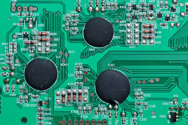
Impedance control is another critical consideration in RF and microwave PCB design.
Variations in trace width, dielectric thickness, copper thickness, layer alignment, or material properties can cause impedance deviations. These deviations may increase reflections and insertion loss, particularly in high-frequency signal paths.
Therefore, impedance requirements should be considered from the PCB design stage and maintained throughout fabrication.
A well-developed PCB Design & Layout process can help coordinate stackup design, trace geometry, component placement, and manufacturability before production begins.
Electromagnetic Compatibility
Radar equipment may operate in complex electromagnetic environments. At the same time, different circuits inside the radar system can interfere with one another.
PCB design and manufacturing should therefore consider:
- Controlled signal routing
- Grounding and return paths
- Appropriate layer stackup
- Separation of sensitive and noisy circuits
- Shielding requirements
- Proper impedance control
- Reduction of unwanted crosstalk
These measures help create a more stable electromagnetic environment for the radar system.
Environmental Reliability
Radar equipment may be deployed in outdoor, industrial, marine, transportation, or other demanding environments. Depending on the application, PCBs may need to withstand temperature variations, humidity, vibration, mechanical shock, and long operating cycles.
Material selection, lamination quality, surface finish, solderability, and structural reliability should therefore be evaluated according to the actual operating environment.
2. Material Selection for Radar High-Frequency PCBs
Material selection has a direct impact on high-frequency electrical performance.
Low-Loss Dielectric Materials
For demanding RF applications, engineers may select specialized high-frequency materials, including PTFE-based materials and other low-loss dielectric systems.
The appropriate material depends on factors such as:
- Operating frequency
- Dielectric constant
- Dissipation factor
- Thermal requirements
- Mechanical requirements
- Layer structure
- Cost and production volume
For certain designs, a hybrid stackup combining conventional FR-4 with high-frequency materials can provide a balance between electrical performance, mechanical characteristics, and manufacturing cost.
Copper and Supporting Materials
Copper quality also influences conductor resistance and high-frequency performance. Copper thickness, surface roughness, plating quality, and trace geometry should be considered together rather than independently.
Other materials, including prepreg, solder mask, bonding materials, and surface finishes, should also be selected according to the PCB’s electrical and environmental requirements.
Consistent incoming material inspection is essential. Material specifications should be verified before production to reduce the risk of electrical or mechanical variation between batches.
3. Advanced Manufacturing Processes for High-Frequency PCBs
The manufacturing process must maintain tight dimensional and structural control to preserve the electrical characteristics defined during PCB design.
Precision Circuit Fabrication
High-density radar boards may require fine-line structures and carefully controlled conductor geometry.
Precise imaging, exposure, development, etching, and plating processes help maintain trace width and spacing while minimizing dimensional variation.
For RF circuits, even relatively small geometric deviations can affect impedance and signal behavior. Process capability should therefore be evaluated against the actual design requirements rather than relying only on nominal specifications.
Accurate Multilayer Lamination
Multilayer radar PCBs require precise layer registration and stable lamination.
Lamination parameters such as temperature, pressure, heating rate, curing time, and cooling conditions can affect:
- Interlayer bonding
- Dielectric thickness
- Layer alignment
- Board flatness
- Electrical consistency
- Long-term reliability
Properly controlled lamination is particularly important when different materials are combined in a hybrid high-frequency stackup.
Surface Finishing
Surface finish affects solderability, connection reliability, corrosion resistance, and the performance of contact areas.
Depending on the application and assembly requirements, finishes such as ENIG or immersion silver may be considered. The selected finish should be compatible with the components, assembly process, environmental conditions, and electrical requirements of the final product.
4. Testing and Quality Control for Radar PCBs
Comprehensive PCB quality control is essential when the PCB is used in a high-frequency system.
Impedance Testing
Controlled-impedance structures can be tested to verify whether fabricated impedance values remain within the specified tolerance.
This provides an important link between the PCB design requirements and actual manufacturing results.
High-Frequency Electrical Testing
For appropriate projects, network analysis can be used to evaluate RF characteristics such as insertion loss and return loss.
These measurements help identify potential issues in high-frequency transmission paths and provide useful data for process verification.
Visual and Automated Inspection
Visual inspection and automated optical inspection can identify manufacturing defects such as:
- Open or short circuits
- Trace defects
- Solder mask problems
- Surface abnormalities
- Registration issues
- Component-related assembly defects
When PCB assembly is included in the project, additional inspection and testing methods can be selected according to product requirements.
GOPCBA provides PCB Assembly services covering prototype, low-volume, and production requirements, allowing PCB fabrication and assembly requirements to be coordinated within a unified manufacturing workflow.
Environmental and Reliability Testing
Depending on the intended application, reliability verification may include temperature cycling, humidity exposure, vibration, mechanical shock, electrical stress, and other applicable tests.
The objective is to verify that the PCB maintains its electrical and mechanical characteristics under expected operating conditions.
5. Performance Advantages of a Well-Designed Radar PCB
Improved Signal Integrity
Low-loss materials, controlled impedance, accurate routing, and stable manufacturing processes can reduce unwanted signal attenuation and reflection.
This provides a more reliable electrical foundation for RF transmission and signal processing.
Support for Multiple Frequency Bands
Modern radar platforms may use different frequency ranges depending on their intended application.
A customized PCB stackup can be developed around the required operating frequency, dielectric properties, transmission-line structure, and system architecture.
In some applications, hybrid material construction can integrate different dielectric systems within a multilayer PCB, helping engineers balance RF performance with mechanical and manufacturing considerations.
Improved Long-Term Reliability
Radar systems may need to operate continuously for extended periods. PCB reliability therefore depends not only on initial electrical performance but also on material stability, interlayer bonding, plating quality, thermal behavior, and manufacturing consistency.
A controlled production process helps reduce variations that could otherwise affect long-term performance.
6. How to Select a High-Frequency PCB Supplier
Choosing the right PCB supplier is an important part of developing radar electronics.
Evaluate High-Frequency Manufacturing Capability
Before placing an order, review whether the supplier can support the required:
- High-frequency materials
- Multilayer construction
- Controlled impedance
- Fine-line fabrication
- Hybrid material stackups
- Surface finishes
- Electrical testing
- Reliability verification
The supplier should also be able to review the design requirements and identify potential manufacturing risks before production.
Define Electrical and Mechanical Specifications
Customers should provide clear requirements for parameters such as:
- Operating frequency
- Dielectric material
- Layer count
- Board thickness
- Copper thickness
- Controlled impedance
- Trace width and spacing
- Via structure
- Surface finish
- Dimensional tolerances
- Environmental requirements
Clear specifications reduce communication gaps and make quality acceptance more objective.
Consider Prototype and Low-Volume Production
For new radar designs, prototypes can help verify the PCB stackup, signal integrity, manufacturability, and assembly process before production quantities increase.
GOPCBA’s Prototype PCB Assembly service can support early-stage product validation, while Low Volume PCB Assembly can help bridge validated prototypes and larger production requirements.
7. Conclusion
High-frequency PCBs play an important role in radar electronics by providing the platform for RF signal transmission, processing, and interconnection.
Reliable radar PCB production requires more than selecting a low-loss material. The entire process—from PCB design and stackup development to material control, precision fabrication, impedance verification, assembly, and reliability testing—needs to work together.
For radar and other RF applications, working with an experienced PCB supplier can help engineers translate electrical requirements into a manufacturable and reliable PCB solution.
GOPCBA provides integrated PCB manufacturing and assembly services for prototype, low-volume, and production projects, helping customers manage PCB fabrication and assembly requirements through a coordinated manufacturing process.