
Relay Control PCB: Isolation, Creepage and Drive Circuits
A relay control PCB looks simple on paper: a logic signal goes in, a coil is energised, a contact closes and a load is switched. What makes it a design problem is that the coil and the contact belong to two different worlds. One is a low voltage circuit that must be protected from the load, and the other may be mains or a high current DC rail that must be kept away from the logic. The board is where that separation is created.
What the Board Contains
At its centre is the relay itself, either an electromechanical device with a coil and a set of contacts or a solid state equivalent with an input and an output stage. Around it are the driver that supplies the coil, the isolation that separates the control side from the switching side, the indicator and the connector, and the protection that keeps a transient on the load from destroying the circuit that controls it.
The layout follows from the physical structure of the relay. Coil terminals are at one end and contact terminals at the other, and the board must maintain the separation between them along the surface, through the air and across the gap wherever the relay itself does not provide it.
Isolation and Creepage
Creepage is the distance along the surface of the board between two conductors, and clearance is the distance through the air. Both are specified by the safety standard that applies to the product, and both increase with the working voltage, with the pollution degree of the environment and with the material group of the laminate. On a relay board the critical distances are those between the coil circuit and the contact circuit and between adjacent contacts.
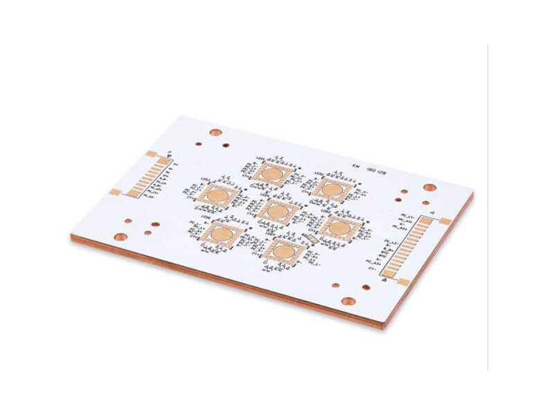
Where the required distance cannot be achieved in the space available, a slot can be routed through the board to increase the surface path without increasing the footprint, and a wider separation on the switching side is always preferable to a marginal one. The dimensions should be checked against the standard rather than copied from a previous design, because the requirement changes with the application and the environment.
Driving the Coil
The coil is an inductor, and interrupting its current produces a voltage spike that will destroy a transistor that is not protected. A flyback diode across the coil is the standard answer: it clamps the spike, at the cost of a slower release because the current circulates through the coil until the energy is dissipated. Where a fast release matters, a diode in series with a Zener diode gives a faster fall at the expense of a higher peak voltage across the switch.
The driver itself has to supply the coil current continuously, which for a small relay is tens of milliamps and for a large one is several hundred. The transistor must be derated for the ambient temperature inside the enclosure, and the trace that carries the coil current sized for the same condition. Drive circuits that use a logic level signal directly should consider the gain of the device at the lowest ambient temperature, which is where a bipolar transistor is weakest.
The Contact Side
On the switching side the constraints change. The traces carry the load current and must be sized for it, with the temperature rise kept within the rating of the laminate and the connector. Where the load is inductive, the contact itself is subject to arcing, and the board should provide a snubber or a varistor close to the contact terminals to reduce the energy the contact has to interrupt.
The relationship between trace width, copper weight, current and temperature rise is set out in trace width and current calculation. Where the current is high, a heavy copper layer or a busbar on the board may be the practical answer, and the connector and the terminal blocks have to be chosen for the same current rather than for the pin spacing alone.
Layout of the Two Sides
The layout should keep the two circuits physically apart and give each its own return path. A common mistake is to route the coil return through the same conductor as the logic return, which injects the coil switching transient into the control ground; the two should meet only at the supply entry point. The same applies to the contact return, which carries the load current and must not share a path with anything sensitive. Keeping the two references apart in this way is the same discipline that applies to any mixed signal layout, and it is described in mixed signal PCB design guidelines.
Where the relay is a solid state device, the internal isolation is defined by the component, but the board still has to respect the creepage and clearance that the standard requires outside the package. The pads and the solder mask openings have to maintain the distance that the package assumes, which is a detail that is easily lost when the footprint is copied from a library. The general rules for pads and their mask openings are described in PCB pad design standards.

Protection and Filtering
Arcing at a contact produces a broad spectrum of interference, and the wiring to the load carries it out of the enclosure. A snubber across the contact, a series inductor or ferrite and a capacitor to chassis at the connector reduce what leaves, and they also reduce what reaches the relay from the load side. The components have to be rated for the working voltage and for the transient energy, which means a mains rated part where mains is switched.
Protection for the control side is equally important. The logic that drives the relay is often connected to a network or to a cable that leaves the enclosure, and a transient arriving on that path should be clamped at the connector rather than at the integrated circuit. Series impedance followed by a suppressor is the usual arrangement, with the ground connection made to the same reference the logic uses.
Testing and Verification
Verification starts with the isolation. The resistance between the coil circuit and the contact circuit, and between adjacent contacts, is measured at the test voltage that the standard specifies, and the creepage and clearance are confirmed on the artwork. Functional testing then exercises the relay through its range of supply voltage and temperature to confirm that it picks up and releases reliably.
Endurance testing follows the application. A board that switches a lamp once a day has a different requirement from one that switches a motor contactor several times a minute, and the test should reproduce the real duty. Where the load is inductive, the test should use the real load, because a resistive load draws a much easier arc and will make an inadequate snubber design look acceptable.
FAQ
Is a flyback diode always the right choice? It is the simplest protection, but it slows the release. Where the timing matters, a diode with a Zener diode in series releases faster at the cost of a higher voltage across the switch.
Can the coil and contact circuits share a ground? They must be separated so that the load and coil currents do not flow through the sensitive return. Where isolation is required by the standard they must not be connected at all.
How is creepage measured? Along the surface of the board between the nearest points of two conductors, including around the edge of a pad or under a component. A slot in the board increases the path.