Rigid PCB Manufacturing: A Buyer and Engineer Review
Rigid boards carry most of the world’s electronics, yet the quotation rarely shows how the work is controlled. The difference between two suppliers often sits in the details that never reach the summary sheet. Which stackup was agreed, which drill program ran, and what the inspection found all decide the yield. This review walks through rigid PCB manufacturing from the first article upward, so buyers and engineers can compare suppliers on evidence rather than on headline price.
A rigid PCB is built on a solid substrate that holds its shape in normal use. FR-4, woven glass cloth bonded with epoxy resin, remains the common choice for most products. Other laminates such as high-TG, PTFE, ceramic or metal-core materials appear when thermal or electrical demands rise. The base material fixes much of the process window, so the material call belongs in the drawing, not in a side message. Getting that call right early avoids expensive changes later.
What Defines a Rigid Board
Every rigid board carries the same functional layers. The substrate gives mechanical support and electrical insulation. Copper forms the conductive paths. Solder mask protects traces and helps prevent bridges during assembly. A surface finish guards exposed pads and keeps them solderable. Silkscreen adds references, polarity marks and traceability data. Each layer has its own process step and its own inspection point, and a fault in one layer often shows up only at final test.
Layer count separates single-sided, double-sided and multilayer boards. As layers increase, routing density and component count can rise, but so does the demand on lamination and registration. A four-layer board is routine work for most factories. A twelve-layer board with blind and buried vias needs tighter control of layer alignment, resin flow and drill accuracy. Buyers should confirm that the quoted factory actually runs the layer count and via structure the design needs.
Stackup and Material Choices
The stackup sets the electrical and mechanical behavior of the finished board. Signal layers, ground planes and power planes are arranged with dielectric thicknesses between them. Controlled impedance traces depend on that geometry, so the fabricator must build the stackup the designer intended. If a laminate thickness changes, impedance shifts and high-speed links may fail. The approved stackup drawing should be signed off before any panel is cut.
Material selection carries cost and risk together. Standard FR-4 covers most commercial products at sensible prices. High-TG laminates help where heat exposure is constant, such as power sections or automotive boards. PTFE suits high-frequency work, and metal-core boards move heat away from dense components. Each choice changes drilling, lamination and plating parameters, so the material call must reach the process engineer before tooling starts, not after the first panels are built.
Lamination Control and Drilling Risk
Multilayer boards are bonded under heat and pressure. Prepreg resin flows, cures and joins the inner layers into one solid structure. Temperature, pressure, resin content and dwell time all matter. Poor control shows up as voids, resin starvation, layer shift or delamination. These defects are hard to see and expensive to find late. The lamination press record is one of the documents a buyer should request when the design is complex or the application is demanding.
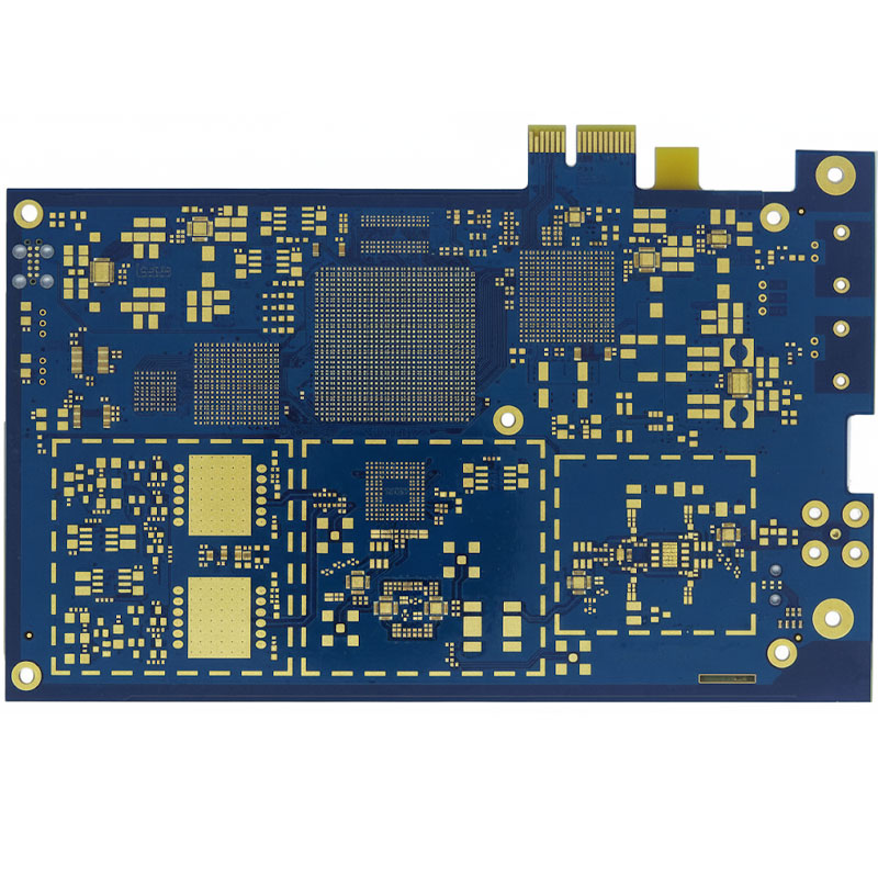
Drilling creates through-holes, vias and other openings. Mechanical drilling handles most holes, while laser drilling serves microvias in HDI designs. Spindle speed, feed rate, tool wear and hole diameter all affect hole quality. A worn bit can smear resin across the copper barrel, and plating then fails to connect. That fault may pass visual checks and fail only in thermal cycling. Drill tool life records and hole inspection data help confirm the process is under control.
Via structures deserve early attention. Blind and buried vias, stacked vias and any-layer HDI all raise the process bar. Back drilling removes unused copper stubs and improves high-speed performance. Via filling supports stacked structures and thermal paths. Each of these features adds steps, and each step adds a place where the process can drift. The design review should confirm that the chosen factory has proven capability for the specific via type, not just for the layer count.
Imaging Etching and Solder Mask
Circuit patterns are defined with photoresist. The resist is coated, exposed through a film or laser image, and developed so that only the intended copper remains protected. Etching then removes the unwanted copper. Trace width and spacing depend on etch control, and over-etching thins traces while under-etching leaves shorts. Etch line parameters are monitored, and coupons on the panel allow the factory to measure the result. After etching, the board is cleaned to remove resist and chemical residue.
Solder mask is applied over the finished copper. Liquid photoimageable mask is common for dense boards because it holds accurate openings around pads. The mask protects traces from solder bridges and shields the surface from contamination. Mask thickness, cure and adhesion all affect performance. A thin or poorly cured mask can blister in reflow or trap moisture. Inspection after mask cure should check for skips, bubbles and misregistration around fine-pitch pads.
Surface Finish and Marking
Exposed copper needs a finish before it oxidizes. HASL and lead-free HASL are common and economical. ENIG gives a flat surface for fine-pitch parts and long storage. OSP suits short-life assemblies, while immersion tin and immersion silver serve specific soldering needs. The right choice depends on component pitch, soldering process, storage time and cost. Buyers should state the finish clearly, because a substitution made quietly can change solderability and shelf life.
Silkscreen adds the information assembly and service teams rely on. Reference designators, polarity marks, pin one indicators, logos and traceability codes all belong on the board. On dense boards, silkscreen must not touch pads or sit under components. Placement accuracy matters, and a shifted legend slows assembly and increases the chance of a wrong part. Clear marking also helps field service identify the board revision, which supports faster diagnosis when a unit returns.
Assembly and Test Coverage
Fabrication ends with electrical test, and most projects then move to assembly. Solder paste printing, component placement and reflow form the joints, and each step feeds the next. A rigid board with a good finish and accurate mask supports a stable print and clean placement. When the project needs turnkey PCB assembly, the fabrication and assembly data should be reviewed together, because pad geometry and stencil design are linked decisions.

Inspection catches defects before they ship, but its real value is feedback. When a joint fails, the engineer learns whether paste volume, placement or the reflow profile caused it. That loop between inspection and process control is what lowers defect rates over time. Boards that pass visual checks still need electrical verification, since a cracked joint or wrong part often shows up only under power. A structured PCBA testing plan covers in-circuit test, functional test and burn-in where the product warrants it.
Prototypes are the cheapest place to find problems. A first small batch reveals pad geometry issues, component tolerances and process behavior before thousands of boards are committed. Teams that invest in rapid PCBA prototyping usually reach volume faster and with fewer surprises. The first article should be measured, recorded and approved, and the approved settings should carry into the production lot. That record is the fastest way to trace a field return months later.
Supplier Checks That Matter
When comparing factories, ask for the documents behind the price. A DFM report, an approved stackup, drill and lamination records, inspection data and test results show whether control exists in practice. Ask how the factory handles engineering questions and how quickly it raises them. A supplier that flags a file problem before tooling saves the buyer far more than a small price difference. The same discipline applies whether the order covers PCB assembly or bare boards only.
Cost depends on size, layer count, material, copper weight, quantity, finish, via technology and tolerances. A quote that lists these factors is easier to compare than a single figure. Confirm what is included, such as electrical test, impedance coupons or first-article reports. Ask about lead time for the actual complexity, not for a simple board. For projects that also need SMT PCB assembly, a single supplier for fabrication and assembly removes handoff risk and keeps one record for the whole build.
The practical takeaway is simple. Agree the stackup, material and finish in writing before tooling. Request the first-article record and keep it with the lot data. Review drill and lamination controls for complex builds. Then compare suppliers on records and communication, not only on unit price. A rigid board that meets its drawing on every lot is worth more than a cheaper board that needs rework, and the documents prove which one you are buying.