Multilayer PCB Manufacturer
High-Quality Multilayer PCBs at Competitive Prices
GOPCBA provides custom multilayer PCB manufacturing for complex electronic applications that require high wiring density, reliable signal integrity, and efficient use of board space. Our capabilities cover a wide range of PCB technologies, materials, layer counts, and interconnection structures. Learn more about our complete PCB manufacturing solutions to find the right manufacturing option for your project.
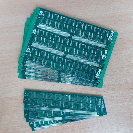
- Rigid, flexible, rigid-flex, HDI, high-TG, high-speed, high-frequency, backplane, embedded, and IC substrate PCBs
- 4–40 layer production and prototypes up to 100 layers
- Blind vias, buried vias, stacked vias, staggered vias, and back drilling
- Conductive and non-conductive via filling and VIPPO
- ISO 9001 and UL-certified manufacturing
- 100% electrical testing, AOI, and visual inspection
As electronic products continue to become smaller and more powerful, conventional single- and double-sided PCBs may not provide enough routing space for increasingly complex circuits. Multilayer PCBs solve this challenge by integrating multiple copper layers into a compact structure, allowing designers to accommodate more components, signal routes, power distribution, and ground planes within a smaller board footprint.
What Is a Multilayer PCB?
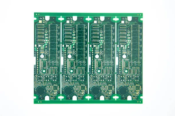
A multilayer printed circuit board (PCB) is a circuit board containing three or more conductive copper layers separated by insulating dielectric materials. In practical manufacturing, multilayer PCBs commonly start at four layers and can extend to much higher layer counts for advanced applications.
Unlike single-sided and double-sided PCBs, multilayer boards contain internal copper layers in addition to the top and bottom outer layers. These internal layers can be used for signal routing, power distribution, and ground planes.
The different conductive layers are interconnected through plated through holes, blind vias, buried vias, and other advanced interconnection structures. The individual layers are bonded together using dielectric cores and prepreg materials to form a mechanically stable PCB stackup.
A typical multilayer PCB structure may include:
- Top copper layer
- Prepreg dielectric
- Inner signal layer
- Core material
- Inner power or ground plane
- Additional core and prepreg layers
- Bottom copper layer
This layered construction provides significantly more routing space without requiring a proportionally larger PCB footprint.
Main Components of a Multilayer PCB
Copper Layers
Copper layers provide the conductive paths required to transmit electrical signals and distribute power throughout the PCB. Internal copper layers can be dedicated to signals, power, or ground planes.
Prepreg
Prepreg is an insulating resin-based material used to bond copper layers and cores together during the lamination process. Its thickness and dielectric properties are important for PCB stackup design and impedance control.
Core
The core is a rigid dielectric material with copper foil laminated to one or both sides. Multiple cores can be combined with prepreg to create the required multilayer stackup.
Copper Foil
Copper foil forms the initial conductive material for the inner and outer layers. Different copper thicknesses can be selected according to current-carrying requirements, thermal performance, and design specifications.
Solder Mask
The solder mask is a protective insulating coating applied over the copper surface. It helps prevent oxidation, contamination, and unintended solder bridges while exposing only the pads and other required areas.
Surface Finish
Surface finishing protects exposed copper and improves solderability and connection reliability. Common options include HASL, lead-free HASL, ENIG, OSP, and other finishes selected according to the application.
Vias
Vias provide electrical connections between different PCB layers. Depending on the design, a multilayer PCB may use through vias, blind vias, buried vias, microvias, stacked vias, staggered vias, and back-drilled vias.
Different Types of Vias in Multilayer PCBs
1. Through Vias
A through via is drilled completely through the PCB and can electrically connect multiple conductive layers from the top surface to the bottom surface.
Through vias are widely used because they are relatively straightforward to manufacture and provide reliable interlayer connections.
2. Blind Vias
A blind via connects an outer layer to one or more internal layers without passing completely through the PCB.
Blind vias are particularly useful for high-density PCB designs because they provide additional routing flexibility while saving board space.
3. Buried Vias
A buried via connects only internal PCB layers and does not extend to either outer surface.
Because buried vias are located entirely inside the board, they can free valuable outer-layer routing space for high-density designs.
4. Stacked Vias
Stacked vias are vertically aligned vias positioned on top of one another across multiple layers.
This structure is commonly used in HDI PCB designs where high-density interconnections are required within a limited board area.
5. Staggered Vias
Staggered vias are offset from one another rather than vertically aligned. They provide an alternative HDI interconnection structure and can offer manufacturing and reliability advantages depending on the stackup.
6. Microvias
Microvias are small-diameter vias typically associated with HDI PCB technology. They are generally formed using laser drilling and allow designers to create very high-density interconnections between adjacent layers.
Advantages of Multilayer PCBs
Multilayer PCBs provide several important advantages for modern electronic products.
1. Smaller PCB Size
Additional internal layers allow designers to route more signals and power connections within the same board area. This makes it possible to reduce PCB size while maintaining or increasing functionality.
2. Higher Component Density
Multilayer construction provides substantially more routing space, allowing more components and interconnections to be integrated into compact electronic products.
3. Improved Electrical Performance
Dedicated ground and power planes can provide shorter return paths and better power distribution. Proper stackup design can also improve signal integrity and help control electromagnetic interference.
4. More Complex Circuit Functions
The additional copper layers make it possible to accommodate high-speed signals, power distribution, sensitive analog circuits, and digital circuits within a carefully engineered stackup.
5. Better Signal Integrity
A properly designed multilayer PCB can maintain controlled impedance, reduce unwanted signal coupling, and provide stable reference planes for high-speed signals.
6. Improved Mechanical Stability
The laminated multilayer structure provides good mechanical rigidity and dimensional stability, which is important for complex electronic assemblies and demanding operating environments.
Disadvantages of Multilayer PCBs
Although multilayer PCBs provide significant performance advantages, they are more complex to design and manufacture than simple single- or double-sided boards.
1. More Complex Manufacturing
Multilayer PCBs require additional processes such as inner-layer fabrication, lamination, sequential drilling, plating, and more extensive inspection.
2. Higher Manufacturing Cost
More materials, manufacturing steps, engineering controls, and inspection processes generally result in higher manufacturing costs compared with simpler PCB structures.
3. Longer Production Time
Complex stackups and advanced interconnection technologies may require additional manufacturing time, particularly for HDI, blind and buried vias, sequential lamination, and other specialized processes.
Multilayer PCB Manufacturing Process
Multilayer PCB manufacturing requires precise process control to ensure layer alignment, electrical performance, dimensional stability, and long-term reliability.
The exact process varies according to layer count, material, via structure, copper thickness, surface finish, and other customer requirements.
1. DFM Engineering Review
Before production begins, engineers review the PCB data to identify potential manufacturing risks.
The DFM review may include:
- Layer and stackup verification
- Trace and spacing checks
- Drill and via analysis
- Annular ring verification
- Copper balancing
- Impedance requirements
- Manufacturing tolerances
- Surface finish requirements
Early DFM analysis helps prevent manufacturing problems and unnecessary design revisions.
2. Material Selection and Cutting
PCB materials are selected according to electrical, thermal, mechanical, and environmental requirements.
Common materials include FR-4, high-TG laminates, high-frequency materials, and other specialized dielectric systems.
The selected cores, copper foils, and prepreg materials are then cut according to the production panel dimensions.
3. Inner-Layer Fabrication
The inner copper layers are cleaned and coated with photoresist. Circuit patterns are transferred onto the copper using imaging technology.
The unwanted copper is then removed during etching, leaving the required circuit pattern.
4. AOI Inspection
Automated Optical Inspection (AOI) compares the manufactured inner-layer pattern with the original design data.
AOI can identify defects such as:
- Open circuits
- Short circuits
- Missing copper
- Excess copper
- Pattern abnormalities
- Dimensional deviations
Additional visual inspection may be performed to verify inner-layer quality before lamination.
5. Lamination
The inner layers, copper foils, cores, and prepreg are precisely stacked according to the approved PCB stackup.
The stack is then subjected to controlled heat and pressure inside a lamination press. The prepreg resin flows and cures, bonding the individual layers into a single multilayer PCB structure.
Layer registration and lamination parameters are critical to the dimensional accuracy and reliability of the finished board.
6. Drilling
Drilling creates the holes required for electrical interconnections and mechanical mounting.
Depending on the design, drilling may include:
- Through holes
- Blind vias
- Buried vias
- Microvias
- Back-drilled vias
Mechanical drilling and laser drilling may be used depending on hole size, depth, and PCB structure.
7. Copper Plating
After drilling, the hole walls are prepared and chemically treated before copper plating.
Copper is deposited onto the hole walls and PCB surfaces to create reliable electrical connections between conductive layers.
Additional electroplating may then increase the copper thickness to the required specification.
8. Outer-Layer Imaging and Etching
The outer copper layers are processed using imaging and etching techniques similar to those used for the inner layers.
The required top and bottom circuit patterns are formed while unwanted copper is removed.
9. Solder Mask and Silkscreen
A solder mask is applied to protect the copper surface and prevent solder bridging during assembly.
Silkscreen or legend printing can then be applied to identify:
- Component reference designators
- Polarity markings
- Part numbers
- Assembly instructions
- Logos and other required markings
10. Surface Finishing
The exposed copper pads receive the specified surface finish.
Depending on the application, surface finishes may include:
- HASL
- Lead-Free HASL
- ENIG
- OSP
- Immersion tin
- Immersion silver
The appropriate finish is selected according to solderability, environmental requirements, contact reliability, and assembly requirements.
11. Electrical Testing
Electrical testing verifies that the manufactured PCB matches the intended circuit connectivity.
Testing methods may include flying-probe testing or fixture-based electrical testing.
These tests help identify:
- Open circuits
- Short circuits
- Incorrect connections
- Electrical continuity problems
12. Routing and Depanelization
The finished PCB panel is separated into individual boards using routing, V-scoring, or other depanelization methods.
The method is selected according to the PCB shape, material, panel design, and customer requirements.
13. Final Inspection and Packaging
Before shipment, finished PCBs undergo final inspection to verify dimensions, appearance, surface finish, markings, and other specified requirements.
Qualified boards are then packaged using appropriate protective materials to prevent moisture, contamination, physical damage, and electrostatic risks during transportation.
Multilayer PCB Design Considerations
A reliable multilayer PCB starts with a properly engineered stackup and manufacturing strategy.
Layer Stackup
The number and arrangement of signal, power, and ground layers directly affect PCB performance.
A well-designed stackup should consider:
- Signal integrity
- Power distribution
- Return current paths
- Impedance control
- EMI performance
- Thermal requirements
- Manufacturability
Controlled Impedance
High-speed digital, RF, and communication circuits may require controlled impedance.
Trace width, copper thickness, dielectric thickness, dielectric constant, and reference-plane configuration should be considered together to achieve the required impedance.
Via Selection
The appropriate via structure depends on routing density, layer count, component pitch, signal speed, and manufacturing capability.
Through vias may be sufficient for conventional designs, while blind vias, buried vias, and microvias can provide additional routing flexibility for high-density applications.
Thermal Management
High-power electronics require careful thermal design. Copper planes, thermal vias, appropriate copper thickness, and suitable materials can help manage heat generated during operation.
EMI and Signal Integrity
Multilayer PCBs can provide excellent EMI performance when the stackup is designed correctly.
Solid ground planes, short return paths, controlled impedance, proper decoupling, and optimized layer transitions can help reduce unwanted electromagnetic interference and signal distortion.
Applications of Multilayer PCBs
Multilayer PCBs are widely used in electronics where space, functionality, signal integrity, and reliability are important.
Typical applications include:
- Consumer electronics
- Computers and servers
- Telecommunications equipment
- Industrial automation
- Medical electronics
- Automotive electronics
- Aerospace and defense electronics
- Networking equipment
- Power electronics
- IoT devices
- Security systems
- High-speed communication equipment
Why Choose GOPCBA for Multilayer PCB Manufacturing?
Selecting the right multilayer PCB manufacturer is critical because complex boards require strong engineering capabilities, reliable process control, and consistent quality management.
GOPCBA provides integrated PCB manufacturing and PCBA services, allowing customers to work with one manufacturing partner from PCB fabrication through assembly and testing. The company website currently presents PCB manufacturing, PCB assembly, component procurement, DFMA, and testing as part of its broader one-stop manufacturing capabilities.
Engineering Support
Our engineering team can assist with DFM review, Gerber verification, stackup considerations, manufacturability analysis, and production optimization.
Flexible Manufacturing
We support different PCB technologies and production requirements, from prototypes and low-volume production to larger production programs.
Quality Control
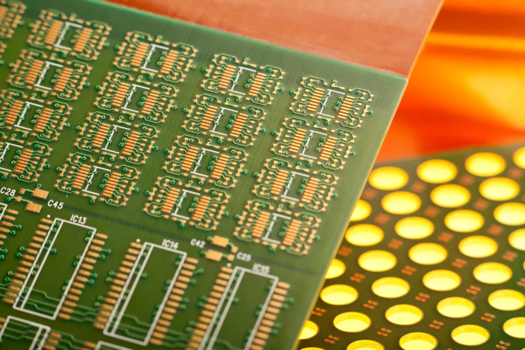
Quality inspection can include AOI, electrical testing, X-ray inspection, visual inspection, and other testing methods selected according to product requirements.
One-Stop Manufacturing
Beyond PCB fabrication, GOPCBA provides PCB assembly, component sourcing, testing, and other electronic manufacturing services, helping customers simplify supplier management and reduce production complexity.
Get a Quote for Your Multilayer PCB Project
Whether you need a conventional 4-layer PCB, a high-density HDI board, a high-TG multilayer PCB, a controlled-impedance high-speed PCB, or a more complex multilayer structure, GOPCBA can help evaluate your design and manufacturing requirements.
Send your Gerber files, stackup requirements, PCB specifications, quantity, and other technical documentation to our engineering team for quotation and manufacturing review.
For project requirements, technical questions, or a custom quotation, please contact GOPCBA and discuss your multilayer PCB requirements with our team.