What Is a Rigid PCB?
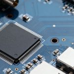
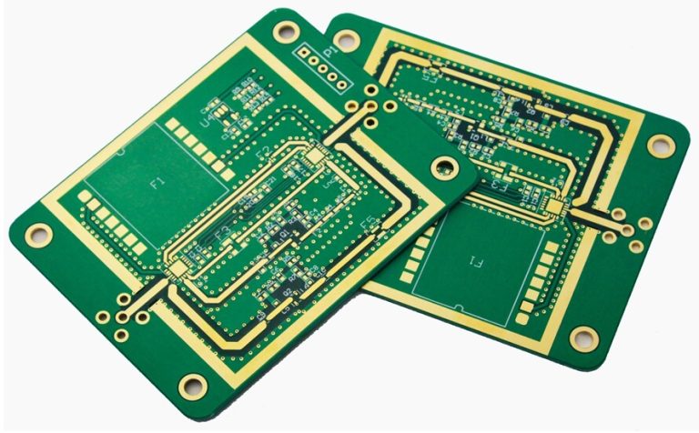
A Rigid PCB is a printed circuit board manufactured with a solid, non-flexible substrate that maintains its shape during normal operation. Unlike flexible PCBs, rigid boards are designed to remain flat and structurally stable after manufacturing. Because of their mechanical strength, reliability, and relatively mature manufacturing technology, Rigid Printed Circuit Board products are widely used in consumer electronics, automotive systems, industrial equipment, medical devices, communications, and other electronic applications.
One of the most commonly used materials for Rigid PCB manufacturing is FR-4, a glass-reinforced epoxy laminate known for its good mechanical strength, electrical insulation, flame resistance, and thermal performance. Depending on the application, other laminate materials may also be selected to meet specific requirements for dielectric constant, thermal expansion, high-frequency performance, heat resistance, or mechanical reliability.
A typical Rigid Printed Circuit Board consists of several functional layers, including the substrate, copper conductors, solder mask, and surface finish. The substrate provides mechanical support and electrical insulation, while the copper layer forms conductive traces, pads, and planes. The thickness of the copper directly affects the board’s current-carrying capability and thermal performance.
Rigid PCBs can be manufactured as single-sided, double-sided, or multilayer boards. As the number of layers increases, designers can achieve higher routing density, more complex circuit structures, better power distribution, and improved signal integrity. However, multilayer designs also require more sophisticated Rigid PCB Manufacturing processes and tighter process control.
Advantages of Rigid PCBs
Rigid PCBs continue to be one of the most widely used PCB technologies because they offer a combination of mechanical stability, manufacturing efficiency, electrical performance, and long-term reliability.
Higher Mechanical Strength
One of the most important advantages of a Rigid PCB is its structural stability. The rigid substrate provides strong mechanical support for electronic components and maintains the board’s shape during assembly and operation.
This makes rigid boards particularly suitable for applications where the PCB must withstand vibration, mechanical stress, repeated handling, or long-term operation.
High Circuit Density
A multilayer Rigid Printed Circuit Board can accommodate multiple signal, power, and ground layers within a relatively compact structure. This allows designers to achieve high circuit density while reducing the overall size of electronic assemblies.
Advanced rigid PCB designs can also incorporate blind vias, buried vias, microvias, fine-pitch components, controlled impedance structures, and other technologies required for high-density electronic products.
Efficient Manufacturing
Rigid PCB Manufacturing is based on mature and highly standardized production technologies. Automated imaging, drilling, plating, inspection, and testing equipment can provide consistent manufacturing quality and high production efficiency.
The standardized nature of rigid PCB production also makes it suitable for both prototype development and high-volume manufacturing.
High Reliability
A properly designed and manufactured Rigid PCB offers excellent dimensional stability and mechanical reliability. The rigid substrate minimizes unwanted deformation and helps maintain consistent component mounting and solder-joint performance.
Material selection, copper thickness, layer structure, thermal management, and surface treatment all contribute to the overall reliability of the finished board.
Flexible Design Options
Although rigid PCBs cannot physically bend like flexible circuits, their internal structures can be customized extensively. Designers can select different layer counts, copper weights, laminate materials, via structures, surface finishes, and impedance configurations according to the application.
This makes Rigid Printed Circuit Board technology suitable for a wide range of electronic products.
Applications of Rigid PCBs
PCB Applications cover almost every major segment of the electronics industry. Because of their mechanical strength, reliability, and manufacturing flexibility, rigid boards are frequently used in the following products and systems:
- Computer motherboards and peripheral equipment
- Servers and data storage systems
- Smartphones and consumer electronics
- Automotive control units and infotainment systems
- Industrial control systems and instrumentation
- Medical equipment and diagnostic devices
- Telecommunications equipment
- Wireless communication systems
- Power supplies and power management equipment
- Aerospace and defense electronics
- Networking equipment and embedded systems
- IoT devices and smart electronic products
For high-performance applications, rigid boards can also be manufactured with high-Tg materials, thick copper, high-frequency laminates, controlled impedance structures, and advanced HDI technologies.
How Are Rigid PCBs Manufactured?
The PCB Manufacturing Process consists of multiple controlled stages. The exact process flow varies according to the layer count, material, copper thickness, design complexity, surface finish, and required electrical and mechanical performance.
Schematic Design and PCB Layout
The PCB Manufacturing Process begins with electronic design. Engineers first develop the schematic to define electrical connections between components. The schematic is then converted into a PCB layout that determines component placement, copper routing, power and ground distribution, via locations, board dimensions, and other physical characteristics.
Designers should consider manufacturing capabilities during the layout stage. Design for Manufacturing (DFM) principles can help prevent issues related to trace width, spacing, drill size, copper distribution, solder mask, and component assembly.
Lamination
For multilayer rigid boards, individual circuit layers are assembled and bonded through the lamination process.
Prepreg materials are placed between copper-clad layers and compressed under controlled temperature and pressure. During heating, the resin softens and flows into the required areas before curing to form a stable multilayer structure.
Precise control of temperature, pressure, resin flow, and lamination time is essential for preventing delamination, voids, thickness variation, and other quality problems.
Photoresist Application and Imaging
A photoresist is applied to the copper surface to define the circuit pattern. The board is then exposed to ultraviolet light through an imaging system or phototool.
Depending on the manufacturing technology, positive or negative photoresist systems may be used. After exposure and development, the required circuit pattern remains protected while unwanted copper areas are prepared for removal.
Modern imaging technologies enable manufacturers to produce fine traces and narrow spacing for high-density PCB designs.
Copper Etching
During the etching stage, unwanted copper is removed from the board while the protected circuit pattern remains.
Common etching chemistry includes copper-compatible acidic or alkaline systems. The etching rate, chemical concentration, temperature, spray pressure, and line speed must be carefully controlled to maintain consistent trace geometry.
After etching, the board is cleaned to remove remaining chemicals and resist materials. Proper etching control is particularly important for fine-line Rigid PCB Manufacturing, where excessive undercutting or over-etching can affect electrical performance.
Drilling
Mechanical drilling is used to create through-holes, mounting holes, and other required openings. CNC drilling equipment can accurately process large numbers of holes according to the PCB design data.
For high-density boards, smaller drill diameters and laser-drilled microvias may be required. Drill parameters such as spindle speed, feed rate, tool geometry, and stack height must be optimized according to the board material and hole size.
Drilling quality directly affects subsequent plating and electrical connectivity.
Plating
After drilling, the exposed hole walls need to be metallized to create electrical connections between PCB layers.
A typical process includes chemical copper deposition followed by electroplating. Copper is deposited onto the hole walls and board surfaces, creating conductive pathways between different layers.
Copper plating thickness must be controlled carefully to meet electrical, mechanical, and reliability requirements.
Solder Mask Application
Solder mask is applied to protect copper traces and reduce the possibility of solder bridges during assembly. It also provides additional protection against environmental contamination and oxidation.
Liquid photoimageable solder mask (LPI) is widely used in modern Rigid PCB Manufacturing. The solder mask is coated onto the board, exposed, developed, and cured to form openings over pads and other areas that must remain accessible for soldering or electrical testing.
Surface Finish
The exposed copper pads require a suitable Surface Finish to protect the copper from oxidation and improve solderability.
Common Surface Finish options include HASL, lead-free HASL, ENIG, immersion tin, and immersion silver. Each finish has different characteristics in terms of solderability, flatness, cost, corrosion resistance, and suitability for fine-pitch components.
For example, ENIG provides a relatively flat surface and is commonly selected for high-density boards and fine-pitch components. HASL remains a cost-effective option for many general-purpose PCB applications.
Selecting the appropriate Surface Finish depends on the assembly process, component package, reliability requirements, storage conditions, and application environment.
Silkscreen Printing
Silkscreen is used to print useful identification information on the PCB surface. This may include component reference designators, polarity indicators, logos, test markings, warning symbols, and other production information.
Clear and accurate silkscreen markings help improve assembly efficiency, inspection, troubleshooting, and product traceability.
Electrical Testing and Final Inspection
After manufacturing, the PCB undergoes inspection and testing to verify that it meets the required specifications.
Depending on the product requirements, testing may include automated optical inspection (AOI), flying probe testing, electrical continuity testing, insulation resistance testing, dimensional inspection, solderability evaluation, and other reliability tests.
Final inspection helps identify open circuits, short circuits, dimensional defects, plating problems, solder mask defects, and other potential issues before shipment.
Key Factors to Consider When Choosing a Rigid PCB
Selecting the appropriate Rigid PCB requires more than simply choosing the number of layers. Several technical factors should be evaluated according to the intended application.
Layer Count
Single-sided and double-sided PCBs are suitable for relatively simple circuits, while multilayer boards are preferred for high-density and complex electronic systems.
Material Selection
FR-4 is suitable for many conventional electronic products, but high-Tg, low-loss, high-frequency, halogen-free, and other specialized materials may be required for demanding applications.
Copper Thickness
Copper thickness should be selected according to current requirements, thermal performance, trace width, and manufacturing capability. High-current applications may require heavier copper.
Impedance Control
High-speed digital and RF circuits may require controlled impedance. In these designs, dielectric thickness, copper thickness, trace width, trace spacing, and material characteristics must be carefully controlled.
Surface Finish
The appropriate Surface Finish should be selected based on soldering requirements, component package, environmental conditions, expected service life, and cost targets.
Manufacturing Capability
The manufacturer’s actual capabilities should be considered during the design stage. Factors such as minimum trace width and spacing, minimum drill size, layer count, copper thickness, registration accuracy, HDI capability, and inspection equipment can directly affect the manufacturability and reliability of the final product.
Why Choose Kingda for Rigid PCB Manufacturing?
Kingda provides professional Rigid PCB Manufacturing services for a wide range of electronic applications. Our manufacturing capabilities can be adapted to different board structures, materials, layer counts, copper thicknesses, surface finishes, and technical requirements.
Diverse Manufacturing Capabilities
Rigid PCBs range from simple single-layer boards to complex multilayer and HDI structures. Kingda supports customized PCB solutions based on the electrical, mechanical, thermal, and manufacturing requirements of different projects.
Whether you need a conventional Rigid Printed Circuit Board or a high-density design with fine traces and advanced via structures, the manufacturing process can be optimized according to your specific requirements.
Competitive Pricing
Kingda combines manufacturing efficiency with flexible production solutions to provide competitive pricing for prototype, small-batch, and volume PCB production.
Our engineering team can review technical specifications and production requirements to help identify practical and cost-effective manufacturing solutions.
Consistent Quality
Quality control is an essential part of Rigid PCB Manufacturing. Kingda emphasizes process control throughout material preparation, imaging, etching, drilling, plating, solder mask application, surface treatment, inspection, and final testing.
By maintaining controlled manufacturing processes and inspection procedures, Kingda works to provide reliable PCBs that meet customer specifications and industry requirements.
Professional Technical Support
PCB manufacturing often requires close cooperation between the designer and manufacturer. Kingda’s technical team can assist with design review, DFM analysis, material selection, stack-up considerations, manufacturing process evaluation, and other technical requirements.
Early communication can help identify potential manufacturing risks before production begins, reducing unnecessary revisions and improving project efficiency.
Reliable Delivery
Delivery time is an important factor in modern electronics development and production. Kingda coordinates engineering review, material preparation, manufacturing, inspection, and shipment to support efficient production schedules.
For projects with urgent requirements, production planning can be evaluated according to the board structure, quantity, materials, and manufacturing complexity.
Conclusion
A Rigid PCB remains one of the most important technologies in modern electronics because of its mechanical strength, reliability, manufacturing efficiency, and design flexibility. From basic single-sided boards to advanced multilayer and HDI structures, rigid PCBs can be customized to meet a wide range of electrical, thermal, and mechanical requirements.
Understanding materials such as FR-4, copper thickness, layer structures, via technologies, and Surface Finish options is essential for achieving reliable PCB performance. At the same time, considering manufacturing capabilities during the design stage can significantly improve product quality and reduce production risks.
With professional engineering support and advanced Rigid PCB Manufacturing capabilities, Kingda can provide customized PCB solutions for consumer electronics, automotive, industrial, medical, telecommunications, and other demanding applications.