Semiconductors, Chips, and Integrated Circuits: Differences, Relationships, Manufacturing Processes, and Applications
Semiconductors, chips, and integrated circuits (ICs) are the fundamental technologies behind modern electronics. They are widely used in smartphones, computers, automotive electronics, industrial equipment, communication systems, artificial intelligence infrastructure, and Internet of Things (IoT) devices.
Semiconductor vs. Wafer vs. Chip vs. Integrated Circuit: Key Differences Explained
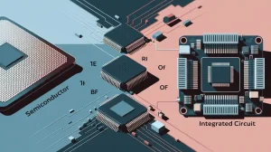
Although the terms semiconductor, chip, and integrated circuit (IC) are often used interchangeably, they actually describe different concepts within the electronics and semiconductor industries. Understanding these differences is essential for engineers, PCB designers, electronics manufacturers, and professionals involved in semiconductor packaging and advanced electronic systems.
In simple terms:
- A semiconductor is a material and technology platform whose electrical conductivity can be precisely controlled.
- A semiconductor wafer is a thin, highly processed substrate used to manufacture integrated circuits and other semiconductor devices.
- An integrated circuit (IC) is an electronic circuit in which transistors and other components are fabricated and interconnected on a semiconductor substrate.
- A chip or die generally refers to an individual piece of semiconductor material separated from a processed wafer. Depending on the context, “chip” may refer to the bare die or, more broadly, to a packaged semiconductor device.
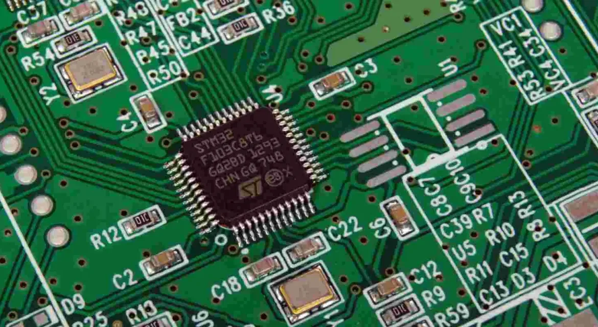
For professionals working in PCB design, IC packaging, semiconductor manufacturing, electronic components, and advanced electronic systems, understanding the relationship between these terms is particularly important. Semiconductor devices eventually need to be packaged and electrically connected to PCBs, which serve as the interconnection platform for complete electronic systems.
Key Takeaways
- A semiconductor is a material whose electrical conductivity falls between that of a conductor and an insulator. Silicon is the most widely used semiconductor material.
- A wafer is a thin slice of semiconductor material that serves as the manufacturing platform for integrated circuits and other semiconductor devices.
- An integrated circuit (IC) integrates large numbers of transistors and other electronic components into a compact semiconductor structure.
- A chip or die is the physical semiconductor unit obtained after the wafer has been processed and separated into individual units.
- A typical semiconductor manufacturing flow is: semiconductor material → wafer fabrication → IC fabrication → wafer testing → wafer dicing → chip packaging → final testing.
- PCB technology connects packaged semiconductor devices and other electronic components to create a complete electronic system.
- Advanced semiconductor packaging and high-density PCB technology are becoming increasingly important for artificial intelligence, 5G, automotive electronics, high-performance computing, data centers, and other demanding applications.
1. What Is a Semiconductor?
A semiconductor is a material whose electrical conductivity is between that of a conductor and an insulator. More importantly, its electrical properties can be precisely controlled through factors such as doping, temperature, electric fields, and light.
Silicon (Si) is the most widely used semiconductor material because of its excellent electrical characteristics, thermal stability, abundant raw materials, relatively low cost, and highly mature manufacturing ecosystem.
Other semiconductor materials are also important for specialized applications, including:
- Germanium (Ge)
- Gallium arsenide (GaAs)
- Silicon carbide (SiC)
- Gallium nitride (GaN)
The unique properties of semiconductor materials allow engineers to manufacture a wide range of electronic devices, including transistors, diodes, sensors, power devices, memory devices, and integrated circuits.
Common Semiconductor Materials
| Semiconductor Material | Key Characteristics | Typical Applications |
|---|---|---|
| Silicon (Si) | Mature technology, stable performance, cost-effective | CPUs, MCUs, memory, power electronics |
| Germanium (Ge) | High carrier mobility | Specialized semiconductor devices |
| Gallium Arsenide (GaAs) | High-frequency and high-speed performance | RF, wireless communications, satellite systems |
| Silicon Carbide (SiC) | High-voltage, high-temperature capability | EVs, inverters, power electronics |
| Gallium Nitride (GaN) | High-frequency operation and high power density | Fast chargers, RF systems, power supplies |
It is important to understand that a semiconductor and a chip are not the same thing.
The term semiconductor primarily refers to a class of materials and the technologies based on their controllable electrical properties. A chip, by contrast, is a physical semiconductor component manufactured using these materials and semiconductor fabrication processes.
2. What Is a Semiconductor Wafer?
A semiconductor wafer is a thin, highly polished slice of semiconductor material that serves as the fundamental substrate for semiconductor manufacturing.
In conventional silicon-based manufacturing, extremely high-purity silicon is processed into a single-crystal ingot. The ingot is then sliced into thin wafers, followed by grinding, polishing, cleaning, and surface treatment.
The resulting wafer provides a highly uniform and extremely flat surface on which manufacturers can build complex electronic structures.
During semiconductor fabrication, wafers undergo repeated manufacturing processes such as:
- Photolithography
- Thin-film deposition
- Etching
- Ion implantation
- Chemical mechanical planarization (CMP)
- Metallization
- Wafer cleaning
- Inspection and metrology
Depending on the wafer diameter, die size, and device design, a single wafer may contain dozens, hundreds, or even thousands of individual semiconductor dies.
Wafer vs. Chip
The difference can be summarized simply:
Wafer = Manufacturing substrate
Chip / Die = Individual semiconductor unit separated from the processed wafer
This distinction is important because integrated circuits are fabricated across the wafer before the wafer is diced into individual dies.
Modern semiconductor manufacturing commonly uses 200 mm and 300 mm wafers, with 300 mm wafers widely used for high-volume manufacturing because their larger surface area can improve production efficiency and reduce the cost per die.
3. What Is an Integrated Circuit (IC)?
An integrated circuit (IC) is a miniature electronic circuit in which a large number of electronic components are fabricated and interconnected within a semiconductor substrate.
These components may include:
- Transistors
- Resistors
- Capacitors
- Diodes
- Interconnects
- Logic circuits
- Memory cells
- Analog circuits
- Input/output circuits
Modern integrated circuits can contain millions, billions, or even more transistors, depending on their architecture, process technology, and application.
By integrating numerous electronic components into a compact semiconductor structure, ICs provide significant advantages in:
- Processing performance
- Functional density
- Power efficiency
- Reliability
- Miniaturization
- Manufacturing scalability
Integrated circuits are used in virtually every modern electronic system.
Central Processing Units (CPUs)
A central processing unit (CPU) executes instructions and performs general-purpose computing operations. CPUs are widely used in computers, servers, industrial equipment, and embedded systems.
Graphics Processing Units (GPUs)
A graphics processing unit (GPU) is optimized for highly parallel workloads, including graphics rendering, artificial intelligence, machine learning, scientific computing, and large-scale data processing.
Microcontroller Units (MCUs)
A microcontroller unit (MCU) integrates a processor core, memory, timers, communication interfaces, and other peripherals into a single IC. MCUs are widely used in embedded systems, consumer electronics, industrial automation, automotive electronics, and IoT devices.
Memory ICs
Memory devices such as DRAM and NAND flash are designed to store and retrieve digital information. They are essential components in computers, smartphones, data centers, automotive systems, and consumer electronics.
Power Management ICs
A power management integrated circuit (PMIC) manages functions such as power conversion, voltage regulation, battery management, power sequencing, and power distribution.
PMICs are especially important in portable electronics, smartphones, computing platforms, automotive electronics, and industrial equipment.
Communication ICs
Communication ICs are used in technologies such as:
- Wi-Fi
- Bluetooth
- Cellular communications
- Ethernet
- 5G
- Radio frequency (RF) systems
- Satellite communications
These devices enable electronic systems to communicate with other devices, networks, and infrastructure.
4. What Is a Chip?
A chip generally refers to a physical piece of semiconductor material containing an integrated circuit or semiconductor device. In semiconductor manufacturing terminology, the individual piece is commonly referred to as a die.
After semiconductor fabrication is completed, the wafer is electrically tested and then separated into individual dies through a process known as wafer dicing.
A semiconductor die may contain:
- Processor cores
- Memory
- Analog circuits
- Digital logic
- RF circuits
- Power management functions
- Specialized accelerators
- Communication interfaces
- Multiple functional blocks
However, the terms chip and integrated circuit are not technically identical.
An IC primarily describes the integrated electronic circuit and its functionality, while a chip generally refers to the physical semiconductor die containing that circuit.
In everyday electronics terminology, however, the two terms are frequently used interchangeably.
Key point: An integrated circuit is primarily a circuit and functional concept, while a chip generally refers to the physical semiconductor die that contains the circuit.
It is also important to distinguish a bare die from a packaged chip. A bare die is the exposed semiconductor component before packaging, while a packaged IC includes the die, package substrate or lead frame, electrical connections, encapsulation, and external terminals.
5. What Is the Relationship Between Semiconductor, Wafer, Chip, and IC?
The relationship between these concepts becomes easier to understand when viewed through the semiconductor manufacturing process.
A simplified process can be represented as:
Semiconductor material → Wafer → IC fabrication → Wafer testing → Dicing → Individual dies → Packaging → Final semiconductor device
Each stage serves a different purpose.
| Term | What It Is | Primary Role |
|---|---|---|
| Semiconductor | Material and technology platform | Provides controllable electrical properties |
| Wafer | Processed semiconductor substrate | Provides the manufacturing platform |
| Integrated Circuit (IC) | Integrated electronic circuit | Performs specific electronic functions |
| Chip / Die | Individual semiconductor unit | Contains the fabricated circuit |
| Package | Protective and electrical interface structure | Protects the die and connects it to the external system |
| PCB | Printed circuit board | Interconnects packaged components within an electronic system |
This distinction becomes especially important when discussing semiconductor packaging, IC substrates, PCB design, HDI PCB, high-speed PCB, and electronic system integration.
After packaging, semiconductor devices must be electrically and mechanically integrated into larger electronic systems. This is where PCB technology becomes critical.
A high-performance PCB must provide reliable signal transmission, power distribution, thermal management, mechanical support, and electrical interconnection for semiconductor packages and other components.
6. Semiconductor Manufacturing Process
Semiconductor manufacturing is one of the most sophisticated manufacturing processes in the electronics industry.
Modern semiconductor devices may require hundreds or even thousands of individual process steps. Extremely precise control of contamination, temperature, pressure, materials, dimensions, and process parameters is required to achieve high yield and reliable device performance.
A typical semiconductor manufacturing process includes material preparation, wafer fabrication, front-end processing, back-end processing, wafer testing, dicing, packaging, and final testing.
6.1 Silicon Material Preparation
The manufacturing process begins with extremely high-purity semiconductor material.
For conventional silicon-based devices, silicon is refined to a very high level of purity and formed into a single-crystal ingot using processes such as the Czochralski (CZ) method.
The quality of the starting material directly affects device performance, defect density, and manufacturing yield.
6.2 Wafer Manufacturing
The silicon ingot is sliced into thin wafers.
The wafers then undergo several processes, including:
- Wafer slicing
- Grinding
- Lapping
- Polishing
- Cleaning
- Surface treatment
- Inspection
The objective is to produce an extremely flat, clean, and uniform surface suitable for advanced semiconductor fabrication.
Modern semiconductor manufacturing commonly uses 200 mm and 300 mm wafers, with 300 mm wafers widely adopted for high-volume production.
6.3 Photolithography
Photolithography is one of the most critical processes in semiconductor manufacturing.
A layer of photoresist is applied to the wafer surface. A photomask and controlled exposure process are then used to transfer the desired circuit pattern onto the photoresist.
Modern semiconductor fabrication may use:
- Deep ultraviolet (DUV) lithography
- Extreme ultraviolet (EUV) lithography
The ability to accurately define increasingly smaller structures is essential for improving transistor density, performance, power efficiency, and overall semiconductor integration.
As process geometries become smaller, lithography requires increasingly sophisticated equipment, materials, alignment systems, and process control.
6.4 Thin-Film Deposition
After lithography, semiconductor manufacturers deposit extremely thin layers of conductive, insulating, or semiconductor materials onto the wafer.
Common deposition technologies include:
- Chemical vapor deposition (CVD)
- Physical vapor deposition (PVD)
- Atomic layer deposition (ALD)
These processes create the material layers required to form transistors, insulating structures, contacts, and interconnects.
6.5 Etching
Etching selectively removes portions of material to create the desired semiconductor structures.
Etching can be broadly classified into:
- Wet etching
- Dry etching
Plasma-based dry etching is particularly important for advanced semiconductor manufacturing because it provides precise control over extremely small structures.
6.6 Ion Implantation and Doping
Ion implantation introduces controlled impurities into semiconductor materials to modify their electrical properties.
By precisely controlling dopant species, concentration, and implantation energy, manufacturers can create the different regions required for transistor operation.
This process is fundamental to controlling the electrical characteristics of semiconductor devices.
6.7 Metallization and Interconnects
Once transistor structures have been formed, multiple layers of metal interconnects are created to electrically connect the devices.
Modern integrated circuits can contain many layers of interconnects.
These structures must provide:
- Low electrical resistance
- High reliability
- Controlled capacitance
- High-speed signal transmission
- Electromigration resistance
Advanced interconnect technology is particularly important for high-performance CPUs, GPUs, AI accelerators, networking chips, and other high-density devices.
6.8 Wafer Inspection and Testing
Before dicing, semiconductor wafers undergo extensive inspection and electrical testing.
Manufacturers evaluate parameters such as:
- Electrical performance
- Leakage current
- Operating voltage
- Frequency
- Power consumption
- Defect density
- Structural integrity
Wafer testing helps manufacturers identify defective dies before packaging, improving production efficiency and reducing unnecessary packaging costs.
7. Semiconductor Packaging and PCB Integration
After wafer fabrication and testing, the wafer is diced into individual dies. The dies are then packaged to provide mechanical protection, thermal management, and electrical connections.
Common semiconductor packaging technologies include:
- QFN
- QFP
- BGA
- CSP
- Flip-chip
- WLCSP
- 2.5D packaging
- 3D packaging
- Chiplet-based packaging
Advanced packaging is becoming increasingly important as semiconductor performance continues to increase.
For example, flip-chip, 2.5D, 3D IC, and chiplet technologies can provide higher interconnect density and shorter electrical paths between semiconductor dies.
The package must then be connected to the PCB.
This creates an important technology chain:
Semiconductor → Wafer → IC → Die → Package → PCB → Electronic System
The PCB therefore plays a critical role in the final stage of electronic system integration.
For high-speed and high-density applications, PCB design must consider:
- Controlled impedance
- Signal integrity
- Power integrity
- Thermal management
- Crosstalk
- Electromagnetic compatibility (EMC)
- Via design
- Layer stack-up
- High-density interconnects (HDI)
- Material selection
As semiconductor I/O density increases, the requirements for advanced PCB manufacturing and IC substrate technology also become more demanding.
8. Semiconductor vs. Chip vs. Wafer vs. IC: Quick Comparison
| Concept | Definition | Main Function |
|---|---|---|
| Semiconductor | Material with controllable electrical conductivity | Provides the physical basis for semiconductor devices |
| Wafer | Thin semiconductor substrate | Provides the platform for fabricating semiconductor devices |
| IC | Integrated electronic circuit | Performs a specific electronic function |
| Chip / Die | Individual semiconductor unit | Contains the fabricated circuit |
| Package | Protective and electrical interface structure | Connects and protects the semiconductor die |
| PCB | Printed circuit board | Connects semiconductor packages and electronic components |
A simple way to remember the relationship is:
Semiconductor is the material and technology foundation.
A wafer is the manufacturing platform.
An IC is the integrated electronic circuit.
A die is the physical semiconductor unit after wafer separation.
A package protects the die and provides external electrical connections.
A PCB connects packaged semiconductor devices to form a complete electronic system.
9. Why These Differences Matter for PCB Design
The distinction between semiconductors, wafers, chips, ICs, packages, and PCBs is not merely a matter of terminology.
As semiconductor technology advances, the electrical and mechanical requirements placed on PCBs become increasingly demanding.
Modern processors, AI accelerators, networking devices, automotive electronics, and high-speed communication systems may operate at very high data rates while requiring increasingly compact form factors.
This creates new challenges for PCB engineers, including:
- Higher routing density
- More complex layer structures
- Tighter impedance control
- Improved power delivery
- Better thermal performance
- Reduced signal loss
- Lower crosstalk
- More precise manufacturing tolerances
For high-performance electronics, the PCB and semiconductor package must be designed as part of an integrated system rather than as completely independent components.
Technologies such as HDI PCB, high-speed PCB, multilayer PCB, rigid-flex PCB, and advanced substrate solutions can help meet the requirements of modern electronic products.
10. The Growing Importance of Advanced Semiconductor and PCB Technologies
The rapid development of artificial intelligence, 5G/6G communications, electric vehicles, autonomous driving, data centers, edge computing, and high-performance computing is driving demand for increasingly advanced semiconductor and PCB technologies.
AI processors and high-performance computing platforms require extremely high data bandwidth and power density. These requirements place greater demands on semiconductor packaging, IC substrates, power delivery networks, thermal management, and PCB interconnection technology.
For this reason, semiconductor manufacturing and PCB manufacturing are becoming increasingly interconnected.
A modern electronic product can be viewed as a complete technology chain:
Semiconductor Materials → Wafer Fabrication → IC Manufacturing → Die → Advanced Packaging → IC Substrate / PCB → System Integration
Each stage affects the performance, reliability, cost, and scalability of the final electronic product.
Companies such as Kingda can support electronic system developers by providing PCB manufacturing and related PCB solutions for applications that require reliable electrical performance, high-density interconnections, and advanced manufacturing capabilities.
Conclusion
Although semiconductor, wafer, chip, and integrated circuit are closely related terms, they describe different stages or concepts within the semiconductor and electronics industry.
A semiconductor provides the material foundation. A wafer provides the manufacturing substrate. An integrated circuit (IC) represents the electronic circuit fabricated on that substrate. After wafer testing and dicing, the resulting die or chip can be packaged and connected to a PCB as part of a complete electronic system.
Understanding this relationship is essential for engineers and manufacturers working with semiconductor devices, IC packaging, PCB design, and advanced electronic systems.
As semiconductor integration continues to increase, the collaboration between semiconductor manufacturing, advanced packaging, IC substrates, and PCB technology will become even more important.
For applications such as AI computing, 5G communications, automotive electronics, industrial automation, data centers, and high-performance computing, choosing the right PCB technology and manufacturing partner is critical to achieving reliable signal integrity, power integrity, thermal performance, and long-term product reliability.
With the continuous evolution of semiconductor and electronic technologies, advanced PCB manufacturing will remain a key link between semiconductor devices and complete electronic systems.
6.4 Thin-Film Deposition
Thin-film deposition creates extremely thin material layers on the wafer.
Common deposition technologies include:
- Chemical Vapor Deposition (CVD)
- Physical Vapor Deposition (PVD)
- Atomic Layer Deposition (ALD)
These layers may serve as conductors, insulators, barriers, or other functional structures within the semiconductor device.
6.5 Etching
After patterning, selected materials must be removed to create the required structures.
Etching can be performed using:
- Wet chemical etching
- Dry plasma etching
Advanced semiconductor manufacturing requires extremely precise control of etching depth, profile, selectivity, and uniformity.
6.6 Ion Implantation
Ion implantation modifies the electrical properties of selected areas of the semiconductor.
Specific ions are accelerated and implanted into the silicon substrate at controlled energies and concentrations.
This process helps create the different semiconductor regions required to form transistors and other devices.
6.7 Chemical Mechanical Planarization
Chemical Mechanical Planarization (CMP) is used to flatten the wafer surface.
As semiconductor structures become increasingly complex and multi-layered, maintaining a uniform surface is essential for subsequent lithography and deposition processes.
CMP therefore plays an important role in advanced semiconductor manufacturing.
6.8 Metallization and Interconnects
Once transistors and other structures are formed, they must be electrically connected.
Multiple layers of interconnects are created to connect individual transistors and functional blocks.
These interconnect structures enable signals and power to travel throughout the IC.
The design and manufacturing of interconnects are especially important for high-performance processors, memory devices, and other advanced ICs.
7. Wafer Testing and Chip Dicing
After wafer fabrication is completed, the wafer undergoes electrical testing.
Testing helps identify defective dies before they proceed to packaging.
The wafer is then separated into individual dies through:
- Mechanical sawing
- Laser dicing
- Other advanced singulation technologies
Each separated die becomes an individual semiconductor chip.
8. Chip Packaging and Testing
A bare die is usually not ready to be directly installed into an electronic system.
It needs to be packaged to provide:
- Mechanical protection
- Electrical connections
- Thermal management
- Environmental protection
- Compatibility with PCB assembly
Common IC packaging technologies include:
- QFN
- QFP
- BGA
- LGA
- CSP
- Flip-Chip
- Fan-Out Packaging
- 2.5D Packaging
- 3D Packaging
For high-performance semiconductor applications, advanced packaging has become increasingly important.
Technologies such as Chiplet, 2.5D integration, 3D integration, and High Bandwidth Memory (HBM) enable multiple dies to work together within a compact package.
9. Chip Packaging and PCB Integration
After packaging, the IC generally needs to be integrated into a Printed Circuit Board (PCB).
The PCB provides the electrical and mechanical infrastructure required to connect the IC with other components.
A modern electronic system may include:
- CPUs
- GPUs
- Memory ICs
- Power Management ICs
- Communication ICs
- Sensors
- Connectors
- Passive components
- PCB assemblies
The relationship can be summarized as:
Chip → IC Package → PCB → Electronic System
The performance of a complete electronic product depends not only on the chip itself but also on the package, PCB layout, power delivery network, thermal design, and signal integrity.
10. Chip vs. Semiconductor vs. IC: Key Differences
| Comparison | Semiconductor | Integrated Circuit (IC) | Chip |
|---|---|---|---|
| Basic definition | Material and technology | Integrated electronic circuit | Physical semiconductor die |
| Typical example | Silicon, SiC, GaN | CPU, MCU, memory IC | Processor die, memory die |
| Main purpose | Control electrical behavior | Perform electronic functions | Physically implement the IC |
| Relationship with wafer | Material used to make wafers | Fabricated on the wafer | Cut from the processed wafer |
| Packaging required | Not necessarily | Usually packaged for system use | Usually packaged before PCB assembly |
| Application | Semiconductor devices | Computing, memory, control | Electronic products and systems |
11. Common Types of Semiconductor Chips
11.1 Processor Chips
Processor chips perform computational and control functions.
They are widely used in:
- PCs
- Servers
- Smartphones
- Embedded systems
- Industrial computers
11.2 Memory Chips
Memory chips store digital information.
Major categories include:
- DRAM
- NAND Flash
- NOR Flash
- SRAM
Memory performance is particularly important in AI systems, smartphones, servers, and data centers.
11.3 Microcontroller Chips
MCUs integrate computing, memory, and peripheral functions into a compact IC.
They are widely used in:
- Automotive electronics
- Consumer electronics
- Industrial automation
- Smart appliances
- IoT devices
11.4 Power Semiconductor Devices
Power semiconductor technologies are critical for electric vehicles, renewable energy systems, industrial power supplies, and fast chargers.
SiC and GaN are particularly important for applications requiring high efficiency, high switching frequency, or high power density.
11.5 Communication Chips
Communication ICs are used in:
- Wi-Fi
- Bluetooth
- 5G
- Ethernet
- RF systems
- Satellite communications
These devices require careful consideration of high-frequency performance, signal integrity, thermal management, and PCB design.
12. Why Semiconductor Technology Is Important
The development of semiconductor technology directly drives the evolution of modern electronics.
Several major trends are shaping the industry.
Smaller Process Nodes
Smaller transistor dimensions can increase transistor density and improve performance and power efficiency, although the benefits and challenges depend heavily on architecture and process technology.
Higher Integration Density
Modern processors and accelerators integrate enormous numbers of transistors into compact silicon dies.
Higher integration enables more computing capability within a smaller physical footprint.
Advanced Packaging
As transistor scaling becomes increasingly challenging, advanced packaging provides another pathway for improving system-level performance.
Important technologies include:
- Chiplet architecture
- 2.5D integration
- 3D integration
- Hybrid bonding
- Fan-Out Packaging
- High Bandwidth Memory
These technologies can improve bandwidth, reduce interconnect distances, and enable heterogeneous integration.
13. Semiconductor Applications
Semiconductors and ICs are now present in almost every modern electronic system.
Consumer Electronics
Smartphones, tablets, laptops, smartwatches, televisions, and gaming systems use a wide range of semiconductor devices.
Automotive Electronics
Modern vehicles may contain hundreds or even thousands of semiconductor devices.
Applications include:
- Advanced Driver Assistance Systems (ADAS)
- Battery Management Systems (BMS)
- Motor Control
- Infotainment
- Connectivity
- Vehicle Networking
- Autonomous Driving
Industrial Electronics
Semiconductors are essential for:
- Industrial controllers
- Robotics
- Servo systems
- Factory automation
- Power conversion
- Measurement equipment
Communication Equipment
Semiconductors are used extensively in:
- Base stations
- Routers
- Network switches
- Optical communication systems
- Wireless communication equipment
AI and Data Centers
AI accelerators, GPUs, CPUs, memory devices, networking ICs, and high-speed interconnects are forming the hardware foundation of modern AI data centers.
These applications also create increasingly demanding requirements for high-speed PCB, advanced PCB materials, thermal management, power integrity, and signal integrity.
14. Semiconductor Industry Milestones
The semiconductor industry has developed rapidly over the past several decades.
1947 — Invention of the Transistor
The invention of the transistor marked a major milestone in modern electronics and laid the foundation for the semiconductor industry.
1958 — Development of the Integrated Circuit
The integrated circuit made it possible to combine multiple electronic components into a compact semiconductor structure.
1970s — Rapid Development of Microprocessors
The widespread adoption of microprocessors accelerated the development of personal computers and embedded systems.
Modern Era — Advanced Semiconductor Manufacturing
Today, semiconductor technology continues to advance through:
- Advanced process nodes
- EUV lithography
- Chiplet architectures
- Advanced packaging
- 2.5D and 3D integration
- HBM
- AI accelerators
- Wide-bandgap power semiconductors
These technologies are transforming computing, automotive electronics, telecommunications, and industrial automation.
15. Semiconductor, IC, Chip and PCB: How Do They Work Together?
A complete electronic product typically requires multiple layers of technology.
A simplified architecture is:
Semiconductor Material → Wafer → IC → Chip → Package → PCB → Electronic System
Each layer performs a different role.
Semiconductor
Provides the material platform and electrical characteristics.
Wafer
Provides the manufacturing platform for creating semiconductor devices.
IC
Provides the electronic functions and circuit architecture.
Chip
Represents the physical semiconductor die.
Package
Protects the die and provides electrical and thermal interfaces.
PCB
Connects the packaged IC with other components and distributes power and signals.
Electronic System
Combines all components to deliver the final product functionality.
This is why semiconductor manufacturing, IC packaging, PCB manufacturing, and PCB assembly are closely connected within the broader electronics industry.
16. PCB Technology for Semiconductor-Based Electronics
As chips become faster and more powerful, PCB technology must also evolve.
High-performance systems increasingly require advanced PCB technologies such as:
- HDI PCB
- High-Speed PCB
- Multilayer PCB
- Rigid-Flex PCB
- High-Frequency PCB
- High-Thermal-Conductivity PCB
- IC Substrate
- Advanced PCB Assembly
High-speed chips require carefully controlled PCB impedance and routing.
At the same time, high-power semiconductor devices generate significant heat, requiring effective PCB thermal management and system-level cooling solutions.
For applications such as AI servers, automotive electronics, telecommunications, industrial automation, and high-performance computing, the cooperation between semiconductor packaging and PCB design is becoming increasingly important.
Kingda focuses on PCB and electronic manufacturing solutions, supporting customers with PCB technologies designed to meet the requirements of modern electronic systems, including high-density interconnection, high-speed signal transmission, thermal management, and reliable PCB assembly.
17. Frequently Asked Questions
Is a chip the same as an integrated circuit?
Not exactly.
An integrated circuit (IC) refers to an electronic circuit that integrates multiple components on a semiconductor substrate, while a chip generally refers to the physical semiconductor die containing that circuit.
The two terms are often used interchangeably in everyday conversation, but they have different technical meanings.
Is a semiconductor the same as a chip?
No.
A semiconductor is a type of material and a broader technology category. A chip is a physical semiconductor component manufactured using semiconductor processes.
A simplified relationship is:
Semiconductor → Wafer → IC Fabrication → Chip → Package
Why is silicon widely used in semiconductor manufacturing?
Silicon has excellent semiconductor properties, is widely available, and can be manufactured at extremely high purity.
In addition, decades of investment have created a mature silicon manufacturing ecosystem, making silicon the dominant material for many semiconductor applications.
How many chips can be made from one wafer?
There is no fixed number.
The number depends on:
- Wafer diameter
- Die size
- Wafer layout
- Edge exclusion
- Process yield
- Manufacturing technology
Larger wafers and smaller die sizes can generally increase the number of usable dies produced per wafer, although actual yield depends on many manufacturing factors.
Are all semiconductor materials used to make chips?
No.
Semiconductor materials are also used to manufacture:
- Diodes
- LEDs
- Power devices
- Sensors
- Photodetectors
- RF components
Different materials are selected according to the electrical, thermal, optical, and frequency requirements of the application.
Why do integrated circuits make electronic products smaller?
ICs integrate large numbers of electronic components into a very small semiconductor area.
This reduces the need for separate components and shortens electrical interconnections, allowing electronic systems to become:
- Smaller
- Lighter
- Faster
- More reliable
- More power-efficient
What is the difference between a chip and a PCB?
A chip performs computing, memory, control, sensing, or signal-processing functions.
A PCB provides the physical platform and electrical connections required to integrate chips and other components into a complete electronic system.
In simple terms:
The chip provides functionality; the PCB provides connectivity and system integration.
Conclusion
Understanding the differences between semiconductors, wafers, integrated circuits, and chips is essential for understanding modern electronics.
The relationship can be summarized as:
Semiconductors provide the material and technological foundation. Wafers provide the manufacturing platform. Integrated circuits provide electronic functionality. Chips are the physical semiconductor dies that contain these circuits. Packages protect and connect the chips, while PCBs integrate packaged chips and other components into complete electronic systems.
From silicon purification and wafer manufacturing to photolithography, etching, ion implantation, metallization, testing, dicing, packaging, and PCB assembly, semiconductor products pass through a highly sophisticated manufacturing chain before becoming part of an electronic device.