Sequential Lamination HDI Stackup Design
In a conventional multilayer board every via passes through the whole stack. As density rises, those through vias consume space on every layer they cross, and the space they take becomes the limiting factor in the layout. Sequential lamination solves the problem by building the board in stages, so that a via can connect only the layers it needs to reach.
What Sequential Lamination Is
The process begins with a core that already contains the inner layers. Holes are drilled in that core and plated to form the connections that will eventually be buried inside the board, and the core is then laminated between additional layers. A second drilling and plating step then creates connections from the new outer layers to the inner ones, and the sequence is repeated for each additional pair of layers.
Each lamination step adds a pair of layers at a time in the most common arrangement, which is why HDI stackups are usually described by the number of build up cycles. A single cycle produces a board with blind vias from the outer layers to the first inner layer, while two cycles add another level of blind vias and allow connections that span a different pair of layers.
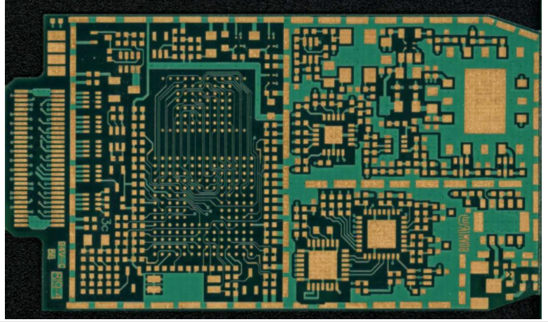
The technique also allows finer features. The dielectric between the build up layers is thinner than in a conventional core, which allows smaller drilled holes and finer lines on the outer layers. The combination of finer geometry and shorter via spans is what makes high density interconnect possible at all.
Blind and Buried Via Structures
A blind via starts at an outer layer and ends at an inner layer without passing through the board. It saves the space that the via would otherwise occupy on the layers it does not reach, which is significant in a dense layout where every layer is crowded.
A buried via connects two or more inner layers and is completely enclosed by the finished board. It is formed before the outer layers are laminated, so it can be placed under surface components without obstructing them, and it does not consume any surface area at all. The choice between the two, and the number of levels that a design should use, is covered in our guide to blind and buried via selection.
Stacked vias, where one via sits directly on top of another, allow a connection to span several layers. They are useful for escaping a dense ball grid array, but they require careful filling and planarisation, because plating over a void produces an unreliable connection. Staggered vias avoid that requirement at the cost of some routing space.
Registration and Layer to Layer Tolerance
registration tolerance is the amount by which one layer can be misaligned with another after lamination, and it is the parameter that governs how much annular ring a design needs. The tolerance accumulates through the process, so a board with two build up cycles has a larger registration budget than one with a single cycle.
The drill to copper position is the second tolerance. The drill that forms a blind via may be offset from the target pad, and the design has to provide enough capture pad to guarantee a connection even at the worst case offset. The fabricator will provide a table of these allowances, and the layout should be drawn to them rather than to the nominal values.
Where the tolerance is tight, a design has to reduce the number of layers it spans or accept a larger pad, which reduces the routing density that the build up was intended to provide. This interaction is why the stackup should be chosen together with the routing strategy rather than before it.
Stackup Planning
The layer stackup determines which via spans are possible as much as it determines the impedance of the signal layers. A stackup with a thin build up layer on the outside gives fine outer routing and good impedance control, while a thick core in the middle provides mechanical rigidity. The arrangement of signal, ground and power layers, described in our guide to layer stackup design, is constrained further by the need to place the buried via connections between the right pairs of layers.
Drawing the stackup before the layout, with each via span marked, prevents the situation where a critical connection turns out to be impossible. The drawing should show the drill spans, the target layers for each signal group and the reference plane for each signal layer, so that the impedance and the via structure can both be verified before routing begins.

Design Rules and Fabrication Constraints
Design rules for a sequentially laminated board are more numerous than for a conventional one, and they differ between fabricators. The minimum blind via diameter is usually larger than the minimum through via diameter because of the aspect ratio of the drilled hole, and the capture pad has to grow accordingly. The minimum dielectric thickness is set by the material and by the need to avoid arcing between the layers.
Copper filling of the vias is required wherever a via is stacked or where a component is placed over it. Filling and planarisation add process steps and cost, and the fill material has a different thermal expansion from the copper, which is one reason why stacked vias in a high temperature application need to be evaluated carefully.
Design rule checks have to be run against the actual fabrication rules rather than against a generic set. The checks that catch the most problems are the via span check, which confirms that every via connects only the layers it is allowed to, and the registration check, which confirms that the pads are large enough for the accumulated tolerance. The documentation practices used for HDI data are described in HDI CAM methods.
Cost Drivers and Yield
Each lamination cycle adds cost, and the increase is not linear. The second cycle is significantly more expensive than the first because the panel has already been through the process once and the yield of the remaining steps applies to a more valuable panel. A design should therefore use the minimum number of cycles that allows the routing to be completed.
Material utilisation matters as much as the number of cycles. The build up material is applied across the whole panel, and a design that uses only part of the available outer layer density pays for the full cost. Reviewing whether the density really needs the finer rules is worth doing before committing to the stackup.
Yield falls as the number of process steps rises, and the fall is what makes low volume sequential lamination expensive. The fabricator can provide a realistic yield estimate for a given design, and it should be obtained before the design is released rather than after the first order.
Verification and Documentation
Verification of a sequential lamination design begins with the cross section. A coupon built alongside the board is sectioned and inspected under a microscope to confirm that the dielectric thicknesses, the via spans and the plating are as designed. This is the only way to see the internal structure, and it is standard practice for a new stackup.
Coupon testing also covers the electrical parameters. Impedance coupons confirm that the trace geometry produces the intended impedance with the actual materials, and they should be measured before the production order rather than assumed from the stackup calculation.
The documentation should describe the stackup layer by layer, name the via spans and their target layers, and state the tolerance that the design has assumed. A fabricator who receives that information can point out conflicts before the panels are built, and the resulting design is faster to manufacture and less likely to require a revision.
FAQ
How many lamination cycles do I need? The minimum that allows the routing to close. One cycle handles most dense designs, while two or more are reserved for very high density boards with fine pitch devices.
Can a blind via be placed under a component pad? Yes, provided it is filled and planarised, and provided the fabricator supports the process. Stacked vias carry additional requirements for filling.
What is the biggest design mistake with HDI? Choosing the stackup before understanding the fabrication tolerances, which leads to a layout that cannot be produced with an acceptable yield.