Signal Routing Order: Prioritizing Nets on Dense Boards
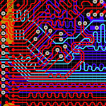
On a dense board, the order in which nets are routed matters as much as the routing itself. A clock line routed after the data bus has to detour around obstacles that the bus already occupied, and the resulting length, layer changes, and proximity to aggressors are all worse than they needed to be. Treating signal routing order as a planned decision, and pairing it with deliberate net prioritization, is one of the cheapest ways to improve signal quality on a board that has no spare space.
The rules below come from high-reliability board practice, where the routing plan is reviewed before any trace is drawn. They apply equally to commercial designs that have run out of margin.
Placement Rules That Make Routing Order Possible
Routing order can only be executed if placement leaves room for it. Components should be packed densely enough to keep interconnections short, but not so densely that sensitive nets have no escape path. Devices that have connections off the board belong near the connectors, arranged in the order of the interface they serve, so that the interconnection pattern is short and parallel rather than crossing the whole board.
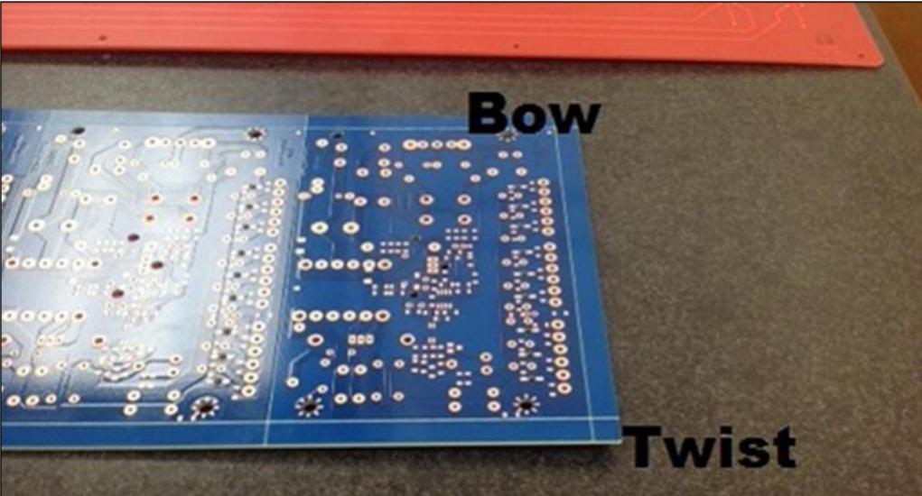
Grouping follows signal behavior rather than schematic page. Devices are partitioned by logic level, edge rate, noise tolerance, and switching behavior, and noisy groups are separated from sensitive ones. Heat-producing parts are distributed so that the board does not develop a hot region, and they are placed away from temperature-sensitive devices, with airflow or heat-spreading area reserved where needed. Heavy components belong near the mounting points, where the board is stiffest, rather than at the center of an unsupported span.
The placement review should also confirm that assembly, test, and repair access survives the floorplan. A board that cannot be probed or reworked will be expensive to debug regardless of how well it routes.
Establish the Routing Area and Edge Clearance
Before routing, define the area in which conductors may exist. Copper, including planes and pours, should stay at least 1.25 mm inside the board outline so that profile machining cannot damage it; that 1.25 mm is the minimum board edge clearance for an inner layer. Where the board runs in a guide slot, surface conductors should stay at least 2.54 mm away; if the slot is intended to provide a ground connection, the border itself should be a ground conductor rather than bare laminate.
Structural features define keep-outs that must be respected as firmly as the outline. Every cutout, slot, and tooling hole needs a routing exclusion zone, and the mechanical drawing’s own keep-out requirements apply as well. Violating them produces either a trimmed trace or a board that will not fit the enclosure.
What Determines the Routing Sequence
The order is set by sensitivity, not by convenience. Nets that are most easily disturbed, or whose delay matters most, are routed while the board is still empty, so that they can take the direct path and stay on a single layer for as long as possible. The practical sequence is: low-level analog signals first, then nets that are especially sensitive to crosstalk, then clock signal nets, then delay-critical buses that require matched lengths, then general-purpose signal routing, and finally static or non-critical connections.
Within each category, the net with the shortest allowable length should be routed first, because it has the least freedom. In practice this means the routing priority is often determined by the length budget rather than by the net class, and the two are reconciled before the first trace is laid.
The same sequence should be respected across revisions. If a board is re-routed after a change, keeping the priority order prevents a sensitive net from losing the path it had in the previous revision.
Wire Width, Spacing, and Uniform Density
Trace width and spacing are chosen from the process capability and the routing demand together. Fine lines allow more channels but raise the chance that a defect will reduce the yield; wide lines are more robust but consume the channel budget. The goal is a uniform density across each layer, with the layers used to a similar degree, because an unbalanced stackup concentrates process risk in one place and often indicates that the routing could be redistributed.
Where a layer has empty regions, adding non-functional pads or short tie traces helps balance plating current and etchant flow. This is a process benefit rather than an electrical one, which is why it is easy to overlook during layout.
Layer Assignment and Orthogonal Routing
Adjacent signal layers should be routed in directions that are orthogonal or at a broad angle to each other wherever possible. The reason is capacitive and inductive coupling between parallel conductors on adjacent layers, which is strongest when the traces run side by side for a long distance. A horizontal-vertical orientation pattern keeps the average parallel run length short.
Crosstalk on the same layer follows the familiar rule: coupling falls as the spacing between traces grows, and it rises with the length over which they run parallel. Where a sensitive net must run alongside an aggressor, inserting a grounded trace between them, or spacing them by at least three times the trace width, reduces the coupled voltage substantially. The mechanisms and the spacing rule are explained in the 3W crosstalk rule.
Separate Power and Ground Structures
Where several supply or ground nets share a layer, the separation between their copper regions should be at least 1 mm. That distance prevents a short caused by a sliver or a plating defect and provides a defined boundary for each net region. Large copper areas larger than about 5 by 5 mm should be broken up with windows, which gives etchants and cleaning chemistry a path and reduces the risk of blistering during thermal exposure.
Where a plane connects to a pad, thermal relief is the standard treatment so that the plane does not conduct heat away during soldering. The same logic applies to ground planning generally: the current path should be deliberate, not the by-product of whichever region of copper happens to be nearest. Return path planning is covered in ground routing and power trace planning.
Controlled Delay and Length Matching
Signals whose timing relationship matters have to be routed with controlled delay, which means the physical length, the layer, and the propagation velocity all count. Two traces of equal length on different layers do not necessarily have equal delay, because the effective dielectric constant differs between a microstrip on the surface and a stripline buried between planes. Matching by length is therefore only valid within a single layer class.
Where a bus requires matching, define the tolerance before routing rather than after, since the tolerance determines how much serpentine length is available. Excess serpentine adds coupling between adjacent turns, so the tuning pattern should use the longest possible segments with the widest practical spacing. The trade-offs are described in serpentine routing and length matching.
Finish With a Review, Not With Completion
The routing is complete when the rules have been verified, not when the last net is connected. A final pass should confirm that the priority nets still keep their direct paths, that no plane has been split by a late addition, that spacing to the board edge is intact, and that thermal reliefs and keep-outs survived the final edits. On a high-reliability board this review is documented, and the documented result is what makes the next revision faster.
FAQ
Should clock nets be routed before or after analog signals? After low-level analog signals, but before high-speed data buses. Analog signals have the smallest amplitude and the least tolerance for coupled noise, so they get the first choice of path. Clocks come next because their edges are fast and their timing budgets are tight.
How do I handle a net that has no satisfactory route left? Revisit placement rather than accepting a poor path. Most unresolvable routing problems are actually placement problems, and moving a connector or swapping two devices usually restores a direct path faster than adding layers or accepting extra vias.
Is it acceptable to route sensitive and noisy nets on the same layer? Yes, provided they are separated by adequate spacing, shielded by an intervening ground trace where necessary, and not run parallel for a significant distance. The risk comes from long parallel runs and from shared reference paths, not from sharing a layer.