Single Layer PCB Fabrication: Process and Where It Wins
A single layer PCB is the simplest board that can be manufactured, and it remains in production in enormous volumes. Lighting drivers, power adapters, simple consumer devices, appliance controls and a long list of industrial modules are all built on one conductive layer, because for those products a second layer would add cost without adding anything the design needs.
This article covers how a single-sided board is made, how the process differs from a multilayer one, and where the construction remains the right choice.
What a Single Layer Board Is
The construction is a rigid substrate with copper on one face, patterned into conductors, covered by a solder mask that exposes the pads, and finished with a protective coating on the copper. Components are mounted on the copper side, and connections that cannot be made on that layer are resolved with wire links or with a redesign of the routing.
The absence of plated through holes is the defining feature. Without plating, a hole cannot connect the two sides of the board electrically, so every connection has to be reachable on the component side. That constraint shapes the layout more than anything else about the construction.
Substrates and Copper Weights
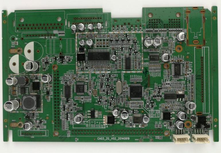
Single-sided boards are commonly built on a paper-based laminate for consumer products, on a glass-reinforced epoxy where mechanical strength or temperature resistance is needed, and on a metal core where the board has to dissipate heat. The paper-based materials are inexpensive and easy to punch, which is why they dominate in high-volume consumer goods.
Copper weight is usually one ounce, though heavier copper is used for power boards. Because the etching tolerance is a fixed absolute figure, heavier copper means a larger minimum feature, and the achievable trace width and spacing on a single-sided power board are noticeably coarser than on a fine-line multilayer board. The trace width and current calculation therefore returns a wider geometry for the same current than it would on a thinner board.
Patterning: Print and Etch
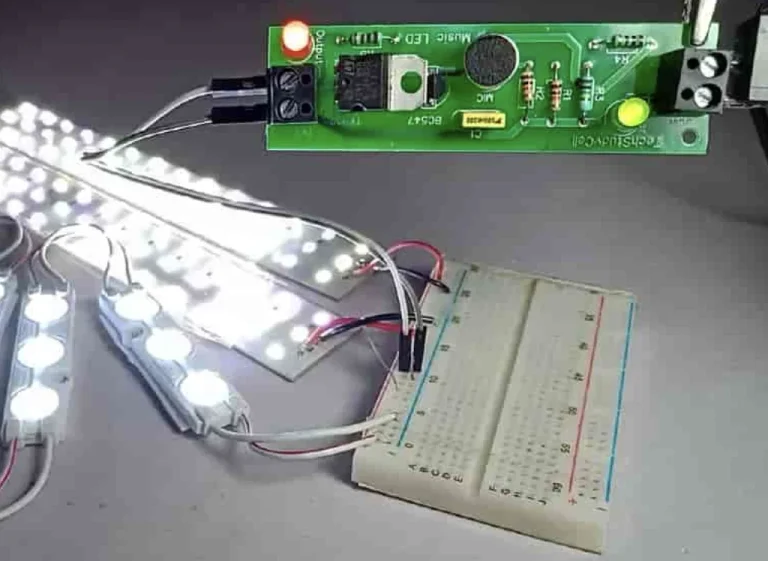
The circuit is formed by printing a resist pattern onto the copper and then etching away the exposed metal. Screen printing is the traditional method and it remains the cheapest for feature sizes above a few tenths of a millimetre, which covers most single-sided work. Where finer features are needed, a dry film resist and a photographic exposure give better resolution at a higher cost.
Because the pattern is produced in a single operation, the tolerance is dominated by the resist printing and the etching rather than by layer-to-layer registration. That is a significant simplification: there is no alignment step to control, no layer-to-layer shift, and no cumulative error. What remains is the etch factor, which sets how much narrower the finished trace is than the printed pattern, and the uniformity of the bath across the panel.
Holes: Drilling Versus Punching
Holes in a single-sided board do not need plating, so they can be made by mechanical punching rather than by drilling. Punching is very fast and very cheap per hole, and it produces clean holes with a controlled diameter, which makes it the preferred method for high-volume consumer boards.
The limitation is the tooling. Each hole size needs a punch and a die, and the tooling cost has to be amortised over the production quantity, so punching only makes sense where the volume is high or the design is stable. Drilling remains the flexible option for low volumes and for hole sizes that change, and it does not require a dedicated tool for each diameter.
Surface Finish and Solder Mask
The solder mask is applied by screen printing, which limits its registration accuracy compared with the photographic process used on multilayer boards. The mask has to clear the pads with enough margin for that tolerance, so the pads on a single-sided board are usually defined a little larger than strictly necessary, and the gap between a pad and its neighbour is a little wider.
The surface finish is chosen for the assembly process. A hot air leveled finish is common because it is cheap and robust, while an organic preservative is used where flatness matters. Because the pads are on one side only, the finish can be applied by a simpler process than on a double-sided board, and the masking of the other side is not required.
Routing on a Single Layer
The routing problem on a single layer is fundamentally about crossings. Two nets that need to cross cannot do so in copper, so the routing has to be arranged so that crossings do not occur, or a wire link has to be added to bridge the crossing. Reducing the crossing count is the central skill of single-sided layout.
Several techniques help. Placing components so that their connections are naturally adjacent reduces the number of nets that have to travel across the board. Choosing a pin assignment for the connector that matches the component layout removes crossings at the interface. Where a crossing is unavoidable, a zero-ohm link or a short jumper wire bridges it, at the cost of an assembly operation. The escape routing rules describe how to arrange the connections leaving a package so that the layer can be used efficiently.
Inspection and Test
Visual inspection is more effective on a single-sided board than on a multilayer one, because every conductor is visible. Automated optical inspection can check the whole pattern, and a human inspector can trace a net by eye. That visibility is a real advantage in a cost-sensitive product, where the test strategy has to be cheap as well as effective.
Electrical test is correspondingly simple. Because there are no buried layers, a flying probe or a simple fixture can reach every net from one side. The test fixture is a single-sided bed of nails, which is cheaper to build and easier to maintain than the double-sided fixture that a multilayer board requires.
Where Single Layer Still Wins
The construction wins wherever the circuit is simple, the volume is high and the cost target is tight. A power supply board, an LED driver, a relay module or a sensor interface with a handful of nets does not need a second layer, and adding one would raise the material cost, the drilling cost and the test cost for no benefit.
It also wins where the board is large and the component density is low, because the cost structure of a multilayer board scales with area while the routing benefit does not. Understanding that cost structure is what allows the decision to be made on evidence rather than by default. Following the manufacturable design rules for the chosen substrate, and planning the routing so that crossings are minimised, usually keeps the design on one layer where a less disciplined approach would push it to two.
FAQ
Can a single layer board have two-sided assembly? Only if the components on the second side are through-hole and their leads pass through the board, because there is no plating to connect to. Surface-mount parts have to be on the copper side.
Why is punching not used for every board? Because each hole diameter needs a dedicated punch and die, and the tooling cost is only justified at high volume. Drilling is slower per hole but requires no dedicated tooling, so it suits prototypes and lower quantities.
How does a single layer board handle a ground plane? The ground is usually a large flooded area on the same layer, connected to the supply return and to the components. There is no separate plane layer, so the return paths share the copper with the signals, which is acceptable at the frequencies these boards normally run at.