Single Sided PCB: Design and Manufacturing Guide
High layer counts and fine lines get the attention, but a very large share of the boards manufactured every year carry their circuit on one layer of copper. A single sided PCB is the cheapest board that can be made, and for a great many products it is also the most appropriate one, because the circuit is simple, the volume is high and the price matters more than the density.
What the Structure Looks Like
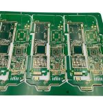
A single sided PCB has one conductive layer on an insulating base, with holes through the board for through hole components and no plated interconnections between layers because there are no other layers. The circuit is completed entirely on that one copper face.
Components mount on the top, and the bottom carries nothing but the substrate and, optionally, printed identification. The absence of plating, multilayer lamination and layer registration removes most of the process steps that make a multilayer board expensive.
Where the Structure Is Competitive
The classic applications are simple ones: power supplies, LED drivers, appliance control panels, toys, chargers and industrial indicator boards. In each case the circuit has relatively few connections, the component count is low, and the product sells in volume.
Cost is the reason. A single sided board uses less material, needs fewer process steps and is easier to test, so the unit price is lower at any quantity. Where the circuit fits on one layer with reasonable routing, adding layers adds cost without adding value.
Layout Rules for One Layer
Routing on a single layer requires planning rather than fixing. The designer has to sequence the connections so that later traces do not block earlier ones, which is the opposite of the multilayer habit of adding a layer when the routing becomes difficult.
Keeping the highest current paths short and direct, grouping components by function and reserving a clear corridor for the supply and return conductors all make the routing feasible. Where the circuit does not fit, the answer is a jumper wire or a second layer, and both should be considered at layout stage rather than discovered during review.
Jumper Wires and Their Cost
A jumper wire carries a connection that the copper layer cannot reach, either as a zero ohm resistor or as an insulated wire placed by the assembly line. It costs money twice: once for the part and once for the assembly operation, which is manual or semi automatic and therefore slower than reflow.
Even so, a jumper wire is often cheaper than moving to a two layer board, particularly in low volumes where the plating and lamination costs dominate. The decision should be made arithmetically, comparing the extra assembly cost against the difference in board price, and the mechanical height that the wire adds has to be acceptable in the enclosure.

Copper Areas and Thermal Behaviour
Single sided boards have no inner planes, so heat has nowhere to spread other than the copper on the component side. A generous copper pour around power devices compensates, and it also reduces the amount of etchant needed, since copper that stays is copper that was not removed.
The pour has to be designed rather than painted in. Areas connected to different nets must be separated by a clear gap, and a large unconnected pour can act as an antenna if it is left floating. Where the pour is connected to supply or ground, the connection must be solid rather than a thin neck that carries the full current.
Surface Finish and Solder Mask
Finish options for a single sided PCB are the same as for any other board. Hot air levelling is the cheapest and is adequate for through hole assembly, while immersion tin and gold finishes suit finer pitch surface mount parts and longer storage.
A solder mask is worth specifying even on the simplest board. It protects the copper from oxidation, prevents solder bridges during wave soldering and reduces the chance of a stray short in service. Where the finish is hot air levelling on a low cost product, the mask is the part worth keeping if only one is affordable.
Design for Assembly
Assembly for a single sided board is usually wave soldering for through hole parts, or reflow followed by wave for a mixed assembly. Both processes put the board through a thermal excursion, so pad size, clearance and thermal relief connections have to suit the process rather than only the electrical requirement, and the pad geometry rules that follow from that are set out in PCB pad design standards.
Clearance around the board edge allows the conveyor to hold the panel without touching components, and a fiducial or two helps an automated line place parts. These are small details, but on a board that will be produced in high volume they decide whether the line runs at speed or stops for adjustments.
Testing and Inspection
Testing a single sided board is simpler than testing a multilayer, because only one layer can carry the circuit and visual inspection is meaningful. Automated optical inspection still applies where the volume justifies it, and electrical test verifies continuity and isolation on every board.
Repair is another practical advantage. A single layer board can be reworked with a soldering iron and a desoldering pump in a way that a fine pitch multilayer cannot, which matters for products where field repair is part of the service model. The trade is that the circuit is more exposed to mechanical damage, so the enclosure and the mounting have to protect it.
In circuit testing becomes harder where there is no internal ground plane, because the reference for measurements is weaker. For simple products a functional test at the end of the line usually gives more useful information than a complex fixture, and it catches assembly faults as well as board faults.
Economic Considerations
Panel utilisation drives cost at every level. A single sided design that nests efficiently on the standard panel size, avoids odd outlines and keeps the drilled hole count low will be cheaper than a more elaborate board of the same area.
The other lever is the order quantity. Because the tooling is minimal, the price per unit falls quickly as quantity rises, and a design that is competitive at ten thousand pieces may be uneconomic at a hundred. Matching the construction to the volume is as important as matching it to the circuit, and the same reasoning about outlines applies in board outline and mounting design.
FAQ
Can surface mount parts be used on a single sided board? Yes, and it is common. The limitation is routing, not assembly, since a dense surface mount circuit often needs a second layer to escape the connections.
Is a single sided board less reliable? Not inherently. Fewer layers mean fewer failure mechanisms, though the absence of a ground plane can make EMC harder to achieve in a noisy product, and the finish choice affects the alloy and joint quality compared in lead-free versus leaded solder.
When should the design move to two layers? When the routing no longer fits with an acceptable number of jumper wires, or when EMC or signal integrity needs a reference plane. On simple products, two layers also allow a much cleaner return path.