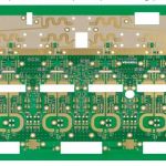
As electronic devices continue to become smaller, lighter, and more highly integrated, PCB designers must achieve higher component density while maintaining soldering quality and long-term reliability. This is especially important for fine-pitch components and BGA PCB assemblies, where solder-pad geometry can directly affect solder-joint formation and mechanical reliability.
Two common approaches are used to define exposed copper solder pads: solder mask defined pad (SMD) and NSMD pad (Non-Solder Mask Defined). Although both structures are widely used in PCB manufacturing, they differ in how the solder mask opening relates to the copper pad.
Understanding these differences is essential for PCB pad design, BGA layout, soldering process control, and reliable PCB assembly.
What Is a Solder Mask Defined Pad?
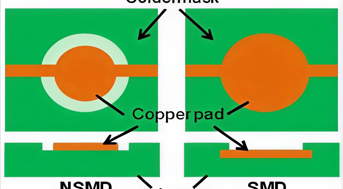
A solder mask defined pad is a PCB pad in which the solder mask opening is smaller than the underlying copper pad. The solder mask partially overlaps the edge of the copper, so the exposed solderable area is determined by the solder mask opening.
In other words:
Copper pad size > solder mask opening
The solder mask therefore defines the effective exposed pad area.
This structure is commonly considered for fine-pitch components and certain BGA pad design applications where mechanical support and pad retention are important.
Because the solder mask overlaps the edge of the copper pad, the copper-to-laminate interface can provide additional mechanical support. This can help reduce the risk of pad lifting during assembly, rework, or repeated thermal cycling.
However, the exposed solderable area is smaller than the total copper pad area. Therefore, the available area for solder-joint formation must be carefully considered during component and PCB design.
What Is an NSMD Pad?
An NSMD pad, or Non-Solder Mask Defined pad, uses a solder mask opening that is larger than the copper pad.
In this structure:
Solder mask opening > copper pad
The solder mask does not overlap the copper pad. Instead, the complete copper pad is exposed, and the solder mask clearance extends around the copper.
The effective pad dimensions are therefore primarily controlled by the copper geometry rather than the solder mask opening.
NSMD pads are widely used for surface-mount components and BGA packages because the exposed copper geometry can provide a relatively large solderable area and greater flexibility for routing between closely spaced pads.
For high-density layouts, this can be particularly useful because the copper pad itself can be kept relatively compact while maintaining sufficient solder-mask clearance.
SMD vs. NSMD: Key Differences
The main difference between the two structures is the relationship between the copper pad and the solder mask opening.
| Feature | Solder Mask Defined Pad (SMD) | NSMD Pad |
|---|---|---|
| Copper pad | Larger than solder mask opening | Smaller than solder mask opening |
| Solder mask | Overlaps copper pad edge | Clears the entire copper pad |
| Exposed copper | Defined by mask opening | Defined by copper geometry |
| Pad retention | Generally stronger edge support | Less mechanical support from solder mask |
| Routing flexibility | May be more limited | Generally better for fine-pitch routing |
| Solderable area | Controlled by mask opening | Controlled mainly by copper pad |
| Typical applications | Fine-pitch and selected BGA designs | BGA, fine-pitch SMT, general PCB assembly |
Neither structure is universally better. The appropriate choice depends on the package manufacturer’s recommendations, PCB fabrication capabilities, soldering process, electrical requirements, and mechanical reliability requirements.
Why Pad Definition Matters in BGA PCB Design
BGA packages contain a large number of solder balls arranged on a compact grid. As the pitch decreases, the available space between adjacent pads becomes smaller.
For this reason, BGA pad design must consider several factors simultaneously:
- Solder-mask registration accuracy
- Copper pad diameter
- Solder-ball diameter
- BGA pitch
- Solder-joint volume
- Via placement
- Trace routing
- Thermal expansion
- PCB warpage
- Reflow soldering conditions
A small dimensional change in the pad or solder mask can significantly affect solder-joint formation when the component pitch is very fine.
Therefore, pad design should not be determined by a single generic dimension. Designers should always prioritize the semiconductor or component manufacturer’s land pattern recommendations and verify them against the PCB manufacturer’s process capabilities.
Advantages of Solder Mask Defined Pads
A properly designed solder mask defined pad offers several potential advantages.
1. Improved Mechanical Pad Support
Because the solder mask overlaps the edge of the copper pad, it can provide additional mechanical support around the pad perimeter.
This can be beneficial when the PCB is exposed to mechanical stress, thermal cycling, or repeated assembly and rework operations.
2. Reduced Risk of Pad Lifting
During soldering and rework, thermal expansion and mechanical forces can place stress on the copper pad.
The additional support provided by the surrounding solder mask may help improve pad retention, particularly in demanding applications.
3. Suitable for Selected Fine-Pitch Applications
SMD structures can be useful when the designer needs tighter control over the exposed solder area.
They may be considered for specific fine-pitch and BGA applications where package recommendations support this structure.
Advantages of NSMD Pads
An NSMD pad also offers several important advantages.
1. Larger Effective Solderable Area
Because the solder mask opening is larger than the copper pad, the entire copper surface is exposed for soldering.
The exposed copper geometry can therefore be more predictable when the solder-mask registration tolerance is taken into account.
2. Greater Routing Flexibility
For dense BGA layouts, compact copper pads can create more routing space between adjacent pads.
This can make it easier to route traces between BGA pads, particularly when combined with fine-line PCB technology and appropriate via structures.
3. Commonly Used for BGA Packages
NSMD pads are widely used for BGA and other surface-mount packages. However, the final pad structure should always follow the component manufacturer’s recommended land pattern.
Solder Mask Opening Design
The solder mask opening is a critical part of PCB pad design.
For an NSMD structure, the opening is intentionally larger than the copper pad to provide clearance around the copper.
For an SMD structure, the opening is smaller than the copper pad, causing the solder mask to overlap the copper edge.
The required clearance depends on several factors, including:
- PCB manufacturer’s registration capability
- Minimum solder-mask web
- Component pitch
- Copper pad size
- Board thickness
- Surface finish
- Assembly process
- Design rules
- Package manufacturer’s land pattern
A common mistake is to apply one fixed solder-mask expansion value to every component. In practice, the appropriate value should be determined according to the PCB manufacturer’s capabilities and the component datasheet.
PCB Pad Size and Spacing
Correct PCB solder pads require an appropriate balance between solderability, electrical clearance, mechanical strength, and routing density.
For fine-pitch components, designers should carefully evaluate:
- Pad diameter or dimensions
- Pad-to-pad spacing
- Solder mask clearance
- Minimum solder-mask web
- Trace width
- Trace-to-pad clearance
- Via-to-pad spacing
- Via diameter
- Copper thickness
The numerical values should not be treated as universal rules. For example, a fixed minimum pad size or a fixed 0.1 mm solder-mask expansion may be unsuitable for some advanced packages.
Instead, designers should follow the package manufacturer’s recommended land pattern and then confirm that the design is compatible with the PCB manufacturer’s manufacturing rules.
Pad Shape Considerations
The shape of the pad can also affect soldering and assembly performance.
Common pad shapes include:
- Round pads
- Square pads
- Rectangular pads
- Oval pads
- Customized package-specific land patterns
For most components, the recommended pad geometry should come from the component manufacturer’s datasheet or land-pattern specification.
Changing the recommended pad shape without validation can affect solder volume, component alignment, solder-joint geometry, and assembly yield.
SMD and NSMD Pad Selection
When selecting between SMD and NSMD structures, designers should evaluate the entire PCB assembly process rather than considering pad geometry alone.
Choose SMD When:
- Additional pad-edge mechanical support is desirable
- The package manufacturer recommends a solder-mask-defined structure
- Pad retention is an important reliability consideration
- The PCB fabrication process can maintain the required mask registration
- The available solderable area remains sufficient for reliable assembly
Choose NSMD When:
- The component land pattern recommends NSMD
- Maximum copper exposure is desirable
- Fine-pitch routing flexibility is important
- The PCB manufacturer can maintain the required solder-mask clearance
- The BGA package is designed around an NSMD land pattern
The final decision should always be based on the component manufacturer’s specifications, PCB fabrication capability, and assembly process requirements.
Via-in-Pad and BGA Pad Design
Via placement becomes particularly important when working with high-density BGA packages.
In advanced BGA PCB layouts, designers may need to place vias close to or directly within component pads. This is commonly referred to as via-in-pad.
However, a via placed directly in a solder pad can allow molten solder to flow into the via during reflow. This can reduce solder volume at the joint and potentially create soldering defects.
For this reason, via-in-pad structures may require appropriate via filling and capping processes.
A typical advanced BGA structure may therefore involve:
BGA pad → filled via → copper cap → microvia or internal routing
The exact structure depends on the PCB stack-up, component pitch, manufacturing process, and electrical requirements.
Kingda can evaluate via-in-pad structures together with pad geometry, layer stack-up, drilling, plating, and filling requirements to improve manufacturing feasibility.
Soldering and Assembly Considerations
Pad geometry is closely connected to the PCB assembly process.
During reflow soldering, solder paste melts and forms the solder joints between the PCB pads and component terminals or BGA solder balls.
Several factors influence the final solder-joint quality:
- Solder-paste volume
- Stencil aperture design
- Pad dimensions
- Component placement accuracy
- Reflow temperature profile
- PCB warpage
- Surface finish
- Solder mask registration
- Component coplanarity
Therefore, even a theoretically correct pad design may produce inconsistent results if the assembly process is not properly controlled.
For high-density PCB assembly, PCB fabrication and SMT process engineering should be considered together.
Surface Finish and Pad Reliability
The surface finish applied to the exposed copper also affects solderability and long-term reliability.
Common PCB surface finishes include:
- HASL
- ENIG
- ENEPIG
- OSP
- Immersion tin
- Immersion silver
The appropriate finish depends on the application, component pitch, storage requirements, assembly process, and reliability requirements.
For fine-pitch BGA applications, surface flatness and consistency are particularly important because uneven or contaminated surfaces can affect solder-joint formation.
Common PCB Pad Design Mistakes
Several common design mistakes can create manufacturing or assembly problems.
1. Using the Same Pad Rules for Every Package
Different components require different land patterns. Designers should not assume that one pad geometry is suitable for every BGA, QFN, QFP, or passive component.
2. Ignoring Solder Mask Registration
The PCB fabrication process has manufacturing tolerances. If the solder-mask opening is designed too close to the copper pad, registration variation may cause partial coverage or insufficient clearance.
3. Placing Unfilled Vias in BGA Pads
An open via inside a solder pad can cause solder wicking during reflow. When via-in-pad is required, an appropriate filling and capping process should be considered.
4. Focusing Only on Copper Pad Size
Reliable assembly depends on more than copper dimensions. Solder paste, stencil design, mask opening, surface finish, component geometry, and reflow conditions must also be considered.
5. Ignoring the PCB Manufacturer’s Capabilities
Advanced PCB pad design should always be checked against the actual fabrication process. Minimum solder-mask clearance, registration accuracy, via filling, copper thickness, and surface-finish capability can vary between manufacturers.
How Kingda Supports Advanced PCB Pad Design
For complex BGA and high-density PCB projects, Kingda can support the design-to-manufacturing process by evaluating critical parameters such as:
- BGA pad design
- Solder mask opening
- Via-in-pad structures
- Microvias and HDI structures
- Fine-line routing
- PCB stack-up
- Copper thickness
- Surface finish
- Solder-mask registration
- PCB manufacturing tolerances
Early DFM evaluation can identify potential pad, spacing, routing, and via-related issues before production.
This is particularly important for high-density boards where a small design change can affect fabrication yield and assembly reliability.
Conclusion
The difference between a solder mask defined pad and an NSMD pad is primarily determined by the relationship between the copper pad and the solder-mask opening.
With SMD, the solder mask overlaps the copper pad, so the solder-mask opening determines the exposed solderable area. With NSMD, the solder mask opening is larger than the copper pad, leaving the entire copper pad exposed.
Neither structure is universally superior. The correct choice depends on the component package, BGA pad design requirements, PCB manufacturing capabilities, soldering process, mechanical reliability, and routing density.
For modern high-density PCB applications, designers should consider pad geometry, solder-mask registration, via structures, surface finish, stencil design, and reflow conditions as one integrated system. By combining accurate PCB pad design with appropriate manufacturing controls and assembly processes, manufacturers can achieve more reliable solder joints, better production yield, and improved long-term PCB performance.
Kingda can help evaluate these factors during PCB design and manufacturing to ensure that the selected pad structure is both technically appropriate and manufacturable.