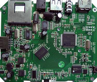
SMT Assembly is one of the most widely used technologies in modern electronics manufacturing. It enables electronic components to be mounted directly onto the surface of a printed circuit board (PCB), providing high production efficiency, excellent assembly density, and consistent manufacturing quality.
Compared with traditional through-hole assembly, SMT Processing can accommodate smaller components and support highly automated production. As electronic products become smaller and more integrated, SMT has become essential for smartphones, consumer electronics, industrial equipment, automotive electronics, communications equipment, medical devices, and other applications.
However, the cost of SMT production is influenced by many factors. Equipment investment is only one part of the overall cost. Component type, PCB design, solder paste printing, placement requirements, inspection, testing, production volume, and quality requirements can all affect the final SMT Assembly Cost.
This article explains the major stages of SMT production and the key factors that influence PCBA manufacturing costs.
What Is SMT Assembly?
SMT Assembly is a PCB assembly technology in which surface-mount components are placed directly onto solder pads on the PCB.
A typical SMT production line may include:
- Solder paste printing
- Solder paste inspection
- Component placement
- Pre-reflow inspection
- Reflow soldering
- AOI inspection
- X-ray inspection when required
- ICT or functional testing
Each stage contributes to the quality, efficiency, and cost of the final PCBA.
A well-designed SMT production process does more than simply place components on a PCB. It must maintain accurate component positioning, consistent solder-joint quality, controlled thermal profiles, and reliable electrical performance.
Key Factors Affecting SMT Assembly Cost
1. Solder Paste Printing
Solder Paste Printing is the first major process in most SMT production lines.
A stencil is used to deposit a controlled amount of solder paste onto the PCB pads. The quality of this process directly affects subsequent solder-joint formation.
Important parameters include:
- Stencil thickness
- Aperture design
- Solder paste type
- Paste storage conditions
- Printing pressure
- Squeegee speed
- Separation speed
- PCB support
- Printing alignment
Solder paste must be stored and handled according to the manufacturer’s specifications. Before printing, it normally needs sufficient time to reach the appropriate working temperature.
Poor printing control can result in insufficient solder, excessive solder, bridging, solder beads, or other assembly defects.
For fine-pitch components such as QFN, BGA, and very small chip components, stencil design and printing accuracy become especially important.
Therefore, controlling Solder Paste Printing is one of the most effective ways to prevent downstream defects and unnecessary rework costs.
2. Solder Paste Inspection
Solder paste inspection (SPI) is used to evaluate solder paste deposition before components are placed.
Modern SPI systems can measure characteristics such as:
- Solder paste volume
- Area
- Height
- Offset
- Shape
- Bridging or insufficient deposits
The major advantage of SPI is early defect detection.
If a printing problem is discovered before component placement and reflow, the PCB can often be corrected before additional manufacturing value is added.
This makes SPI an important part of PCBA Manufacturing quality control. Although inspection adds equipment and operating costs, early defect detection can reduce rework, scrap, and troubleshooting costs later in the production process.
3. Component Placement
Component placement is one of the core stages of SMT Processing.
High-speed placement machines are commonly used for small chip components, while flexible or multifunctional placement equipment can handle larger, irregular, or more complex components.
Component characteristics that can affect assembly cost include:
- Component package
- Component size
- Component height
- Placement accuracy
- Component orientation
- Feeder requirements
- BGA and QFN packages
- 0201 or smaller components
- Number of unique components
- Total placement points
Very small components require greater placement accuracy and more precise process control.
BGA, QFN, fine-pitch ICs, and other high-density packages may also require more demanding inspection and process validation.
The number of placement points is another important cost driver. A PCB containing thousands of components generally requires more machine time than a board with a small component count.
4. Manual Visual Inspection
Manual inspection can complement automated inspection systems, particularly for component orientation, polarity, mechanical conditions, and areas that may require human judgment.
Typical issues that can be identified include:
- Missing components
- Incorrect component orientation
- Incorrect component placement
- Polarity errors
- Damaged components
- Obvious soldering problems
Finding these issues before or immediately after reflow can reduce the cost of subsequent repair.
However, manual inspection should generally be used as a complement to automated inspection rather than as a substitute for appropriate automated process controls in high-volume manufacturing.
5. Reflow Soldering
Reflow Soldering is the process in which solder paste is heated according to a controlled thermal profile until the solder melts and forms reliable electrical and mechanical connections.
A typical reflow profile includes several stages:
- Preheating
- Soaking
- Reflow
- Cooling
The appropriate profile depends on the solder paste, PCB construction, component requirements, and reflow equipment.
Important parameters include:
- Ramp rate
- Soak conditions
- Peak temperature
- Time above liquidus
- Cooling rate
- Temperature uniformity
An improperly controlled profile may cause solder defects, component damage, warpage, voiding, or excessive thermal stress.
For lead-free assembly, thermal requirements are generally more demanding than for traditional leaded solder systems because common lead-free alloys have higher melting temperatures.
Therefore, process engineers must establish the reflow profile according to the specific solder paste and component specifications rather than applying a universal temperature curve.
Efficient Reflow Soldering helps improve first-pass yield and reduce rework.
6. AOI Inspection
AOI Inspection, or Automated Optical Inspection, uses cameras and image-processing algorithms to inspect PCB assemblies.
AOI can identify many visible defects, including:
- Missing components
- Component misalignment
- Incorrect polarity
- Solder bridges
- Insufficient solder
- Excessive solder
- Tombstoning
- Open solder joints
- Incorrect component placement
AOI is particularly useful for high-volume production because it provides consistent inspection coverage and reduces dependence on manual visual inspection.
However, AOI cannot detect every possible defect. Hidden solder joints under BGA components, for example, may require X-ray inspection.
The inspection strategy should therefore be selected according to the PCB design, component package types, product reliability requirements, and production volume.
7. X-Ray Inspection
X-Ray Inspection is commonly used when solder joints or structures cannot be adequately evaluated by optical inspection.
It is particularly useful for components such as:
- BGA
- QFN
- LGA
- Bottom-terminated components
- Other hidden solder joints
X-ray inspection can help identify problems such as solder voids, insufficient solder connections, bridging, and hidden joint abnormalities.
Not every PCB requires 100% X-ray inspection. The appropriate inspection coverage depends on product requirements and risk assessment.
For reliability-critical applications, X-ray inspection can provide valuable information that cannot be obtained through conventional optical inspection alone.
8. ICT and Functional Testing
Electrical testing is an important final step in PCBA Manufacturing.
Depending on the product, manufacturers may use:
In-Circuit Test (ICT)
ICT evaluates specific electrical characteristics of the assembled PCB and can help identify assembly-related problems such as:
- Opens
- Shorts
- Incorrect component values
- Component orientation problems
- Certain soldering defects
Functional Test
Functional testing evaluates whether the completed PCBA operates according to the intended product specifications.
It may involve:
- Power-up testing
- Communication testing
- Input/output verification
- Sensor testing
- Signal testing
- Firmware interaction
- System-level operation
For complex electronic products, functional testing can be especially important because a PCB may pass basic electrical checks while still failing to perform its intended system function.
PCB Design Also Influences SMT Assembly Cost
SMT Assembly Cost is not determined only by the production line. PCB design has a major influence on manufacturing efficiency.
Several design characteristics can increase assembly difficulty:
High Component Density
A highly populated board requires greater placement accuracy and may require more detailed inspection.
Fine-Pitch Components
Fine-pitch QFP, QFN, BGA, and similar packages require more precise stencil and placement control.
Very Small Components
Components such as 0201 packages require appropriate equipment, feeders, PCB support, stencil design, and process control.
Poor Pad and Stencil Design
Improper land patterns or stencil apertures can cause soldering problems and increase rework.
Large Thermal Pads
Large exposed pads may require special stencil aperture designs to control solder volume and reduce voiding or floating.
For this reason, design for manufacturing (DFM) should be considered before production begins.
Production Volume and SMT Assembly Cost
Production volume has a significant effect on unit assembly cost.
Prototype and small-batch production may have higher unit costs because setup, programming, stencil preparation, feeder configuration, engineering review, and testing costs are distributed across fewer boards.
As production volume increases, these fixed costs can generally be distributed across more units.
However, volume should not be evaluated only in terms of unit price. Factors such as component inventory, product life cycle, demand fluctuations, and design changes should also be considered.
A suitable production strategy may include:
- Prototype assembly
- Small-batch production
- Medium-volume manufacturing
- High-volume production
How to Reduce SMT Assembly Cost
Reducing SMT Assembly Cost does not necessarily mean choosing the cheapest assembly service. The better approach is to improve the complete manufacturing process.
Optimize the BOM
Reducing unnecessary component varieties can simplify feeder setup and inventory management.
Standardize Components Where Practical
Using common package sizes and readily available components can improve procurement efficiency.
Optimize PCB Layout
A PCB layout designed for automated assembly can improve placement efficiency and reduce manufacturing problems.
Design an Appropriate Stencil
Stencil thickness and aperture design should be matched to component packages and solder-paste requirements.
Use Appropriate Inspection Coverage
Inspection should be based on product risk and reliability requirements rather than automatically applying the same inspection strategy to every product.
Optimize Panelization
Efficient panel design can improve PCB utilization and reduce handling and machine setup time.
Kingda SMT Assembly Capabilities
Kingda provides SMT Processing and PCBA manufacturing services for prototype, small-batch, and production applications.
Depending on the specific project requirements, Kingda can support assemblies involving:
- Fine-pitch components
- Small chip components
- BGA
- QFN
- High-density PCB assemblies
- Mixed SMT and through-hole assembly
- Automated optical inspection
- X-ray inspection where required
- Electrical testing
- Functional testing
Actual component package limits, PCB dimensions, placement accuracy, and inspection requirements depend on the production equipment and project specifications. These requirements should be confirmed during engineering review before mass production.
Kingda’s manufacturing process focuses on integrating PCB fabrication, assembly engineering, inspection, and testing to help customers achieve consistent PCBA quality and reliable production performance.
Conclusion
SMT Assembly has become a fundamental technology in modern electronics manufacturing because it combines high placement density, automation, production efficiency, and repeatable quality.
The overall SMT Assembly Cost is influenced by many factors, including Solder Paste Printing, component selection, placement complexity, Reflow Soldering, AOI Inspection, X-Ray Inspection, testing requirements, PCB design, and production volume.
For cost-effective and reliable PCBA Manufacturing, the most effective approach is to consider manufacturability from the design stage. Optimizing component selection, PCB layout, stencil design, panelization, inspection strategy, and production parameters can reduce unnecessary manufacturing costs while maintaining the quality and reliability required by the final product.
Kingda can support customers from PCB fabrication through SMT Processing, inspection, testing, and PCBA production, providing an integrated manufacturing solution for different electronic applications.