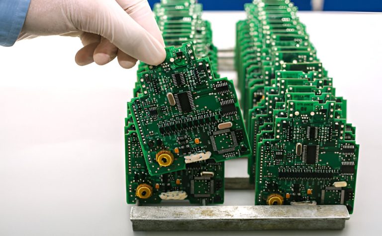
SMT PCB Assembly is one of the most widely used electronic assembly technologies for modern printed circuit boards. It enables electronic components to be mounted directly onto the surface of a PCB, supporting compact designs, high component density, automated production, and consistent manufacturing quality.
Kingda provides PCB manufacturing and assembly solutions for customers with different product structures and production requirements. From prototype development to volume production, a professional SMT Assembly process requires precise equipment, controlled materials, experienced engineering, and systematic quality inspection.
Compared with traditional through-hole technology (THT), SMT allows components to be placed directly on PCB pads without requiring leads to pass through drilled holes. This approach has become particularly important for compact electronic products, high-density circuit boards, and automated manufacturing.
What Is SMT Assembly?
SMT Assembly stands for Surface Mount Technology assembly. It is a PCB assembly process in which electronic components are mounted directly onto the surface of a printed circuit board.
During the process, solder paste is first printed onto designated PCB pads. Automated placement equipment then positions surface-mount components onto the solder paste. The assembled board subsequently passes through a reflow oven, where controlled heating melts the solder paste and forms reliable solder joints.
The basic SMT Assembly process can be summarized as:
Solder Paste Printing → Component Placement → Reflow Soldering → Inspection → Electrical Testing
Unlike conventional THT assembly, SMT does not normally require component leads to pass through the PCB. This makes it possible to achieve smaller products, higher component density, and greater assembly automation.
SMT PCB Assembly vs. Through-Hole Assembly
SMT and THT each have their own advantages and are sometimes used together in the same product.
| Feature | SMT | THT |
|---|---|---|
| Component mounting | Directly on PCB surface | Leads inserted through holes |
| Component density | High | Generally lower |
| PCB space | Efficient | Requires additional space |
| Automation | Highly suitable | Suitable, but some operations may require additional handling |
| Component size | Supports very small packages | Better suited to some large or mechanically demanding components |
| Mechanical strength | Depends on package and solder-joint design | Often advantageous for mechanically stressed components |
| Typical applications | Consumer electronics, communications, industrial electronics | Power components, connectors, transformers, mechanically stressed parts |
Many modern products use a combination of SMT and THT to achieve the best balance between miniaturization, electrical performance, mechanical strength, and manufacturing efficiency.
Benefits of SMT PCB Assembly
PCB Miniaturization
One of the most important advantages of Surface Mount Technology is its ability to support compact PCB designs.
Because SMT components do not normally require through-hole mounting, more components can be placed within a limited board area. Small packages such as QFN, BGA, CSP, and various chip packages allow designers to achieve high circuit density.
This is particularly useful for:
- Wearable electronics
- Portable devices
- Communication equipment
- Medical electronics
- Industrial control systems
- Automotive electronics
- IoT products
Improved Electrical Performance
SMT components can provide shorter electrical connections compared with many traditional leaded components.
Shorter interconnects can reduce parasitic inductance and capacitance, which is particularly useful for high-speed and high-frequency circuits.
However, electrical performance also depends on PCB stackup, trace routing, grounding, component placement, signal integrity, and power distribution. SMT alone does not automatically guarantee superior electrical performance.
Higher Production Efficiency
Automated SMT production lines can place a large number of components at high speed and with high repeatability.
Modern placement machines use vision systems to identify component position and orientation, while automated feeders supply components continuously.
This high level of automation can significantly improve production efficiency, particularly for medium- and high-volume manufacturing.
Consistent Assembly Quality
Automated equipment reduces manual placement variation and allows manufacturing parameters to be monitored and controlled.
When solder paste printing, placement accuracy, reflow profiles, and inspection processes are properly controlled, SMT PCB Assembly can achieve highly consistent production results.
Flexible Component Selection
SMT supports a wide range of component packages and sizes. Designers can combine different package types according to electrical, thermal, mechanical, and cost requirements.
For complex products, SMT can also be combined with THT, selective soldering, or other assembly processes.
Key SMT PCB Assembly Processes
A reliable SMT PCB Assembly process requires careful control at every production stage.
1. Solder Paste Printing
Solder paste printing is the first major assembly operation.
A stencil is positioned over the PCB, and a squeegee moves across the stencil to force solder paste through precisely defined openings onto the PCB pads.
The amount and position of solder paste are critical to solder-joint quality.
Important process parameters include:
- Stencil thickness
- Aperture dimensions
- Squeegee pressure
- Printing speed
- Separation speed
- PCB support
- Paste temperature
- Paste storage and handling
- Stencil cleanliness
Insufficient solder paste can result in weak solder joints, while excessive paste can increase the risk of solder bridging.
For fine-pitch components, stencil design becomes particularly important. Aperture reduction and other stencil-engineering techniques may be used when necessary.
2. Component Pick and Placement
After solder paste printing, automated pick-and-place machines position components onto the PCB.
A typical placement system includes:
- Component feeders
- Placement heads
- Nozzles
- Vision systems
- PCB support mechanisms
- Motion-control systems
The vision system identifies PCB fiducials and component features to improve placement accuracy.
Placement accuracy is essential for fine-pitch devices. Component misalignment can result in insufficient pad overlap, solder bridging, open joints, or other assembly defects.
3. Reflow Soldering
Reflow Soldering is the primary soldering method used in SMT production.
After component placement, the PCB passes through a controlled reflow oven. The temperature profile normally includes several stages, such as preheating, thermal soaking, reflow, and cooling.
The objective is to activate the flux, melt the solder alloy, form reliable solder joints, and cool the assembly under controlled conditions.
A typical reflow profile should be developed according to the solder-paste manufacturer’s specifications and the thermal characteristics of the PCB assembly.
Important parameters include:
- Preheat rate
- Soak temperature
- Time above liquidus
- Peak temperature
- Cooling rate
- Temperature uniformity across the PCB
Poorly controlled reflow can result in insufficient soldering, component damage, solder voids, tombstoning, or other defects.
Nitrogen may be used in some reflow processes when reduced oxidation is beneficial, but the appropriate atmosphere depends on the solder paste, component requirements, PCB finish, and production process.
4. AOI Inspection
AOI Inspection, or Automated Optical Inspection, uses cameras and image-processing algorithms to inspect assembled PCBs.
AOI can identify many visible assembly problems, including:
- Missing components
- Incorrect components
- Component misalignment
- Polarity errors
- Solder bridging
- Insufficient solder
- Excess solder
- Visible solder-joint abnormalities
AOI programs must be properly developed and maintained. Calibration, lighting conditions, inspection thresholds, and regular equipment maintenance are important for minimizing false calls and missed defects.
5. X-Ray Inspection
X-ray inspection is particularly useful for components and solder joints that cannot be adequately inspected from the surface.
It is commonly used for packages such as BGA, QFN, and other hidden-joint components.
X-ray inspection can help identify:
- Solder voids
- Open solder joints
- Bridging
- Insufficient solder
- Misalignment
- Internal structural abnormalities
Both 2D and 3D X-ray systems may be used depending on the inspection requirements.
6. Electrical Testing
Electrical testing verifies whether the assembled PCB performs according to its electrical requirements.
Common methods include:
In-Circuit Test
ICT uses a fixture and test points to measure electrical characteristics and identify certain assembly or component-related faults.
ICT can be highly effective for stable, high-volume products where a dedicated test fixture is economically justified.
Flying Probe Test
Flying probe testing uses movable probes to contact designated test points.
It provides greater flexibility and is often useful for prototypes, low-volume production, and products that change frequently.
Functional Testing
Functional testing evaluates the assembled PCB under conditions that simulate its intended operation.
This may include powering the board, communicating with external equipment, measuring outputs, checking interfaces, and verifying key operating functions.
Common SMT Assembly Defects
Achieving defect-free production is the goal of every PCB Assembly process. However, miniaturization, fine-pitch components, complex layouts, and increasing component density can make SMT manufacturing more demanding.
Insufficient Solder
Insufficient solder occurs when the amount of solder deposited or transferred to a joint is inadequate.
Possible causes include:
- Insufficient solder-paste volume
- Poor stencil design
- Printing misalignment
- Poor pad design
- Inadequate wetting
- Incorrect reflow conditions
Insufficient solder can reduce mechanical and electrical connection reliability.
Tombstoning
Tombstoning occurs when one end of a small two-terminal component lifts from the PCB pad during reflow, leaving the component standing vertically.
It can be caused by unbalanced wetting forces between the two pads, uneven solder-paste deposition, pad-design differences, component placement errors, or an unsuitable thermal profile.
Optimizing pad geometry, solder-paste deposition, component placement, and reflow conditions can reduce tombstoning risk.
Solder Bridging
Solder bridging occurs when molten solder connects two adjacent conductive pads that should remain electrically isolated.
It can be caused by:
- Excessive solder paste
- Incorrect stencil apertures
- Fine-pitch spacing
- Component misalignment
- PCB pad-design issues
- Improper reflow conditions
Solder bridges can create electrical shorts and therefore require effective inspection and process control.
Solder Balls
Solder balls are small, unwanted spheres of solder that may remain near solder joints after reflow.
Potential causes include solder-paste characteristics, moisture, excessive paste deposition, printing conditions, component placement, and reflow parameters.
If solder balls are located in electrically sensitive areas, they can potentially cause shorts or reliability issues.
Component Misalignment
Components may shift during placement or reflow.
Possible causes include placement inaccuracies, uneven solder-paste distribution, insufficient PCB support, component package issues, or unbalanced thermal conditions.
Accurate fiducial recognition, stable placement parameters, and proper stencil design help reduce this type of defect.
Solder Voids
Voids are gas-filled areas within a solder joint.
Some degree of voiding can occur naturally during reflow, but excessive voiding can reduce the effective solder-joint area and may affect thermal or mechanical performance.
The acceptable void level depends on the component, application, solder alloy, design requirements, and relevant specifications.
Factors Affecting SMT Assembly Quality
PCB Design
A good PCB Design should consider SMT manufacturing requirements from the beginning.
Designers should pay attention to:
- Component spacing
- Pad geometry
- Fiducial placement
- Solder-mask design
- Thermal pads
- Fine-pitch routing
- Test-point accessibility
- Component orientation
- DFM requirements
Design-for-manufacturing review can identify potential assembly problems before production begins.
Stencil Design
Stencil design directly affects solder-paste deposition.
Stencil thickness and aperture dimensions should be selected according to component package requirements. Fine-pitch devices and thermal pads may require specially optimized aperture patterns.
Component Quality
Component quality can affect placement, solderability, electrical performance, and long-term reliability.
Manufacturers should use components that meet the project’s specifications and maintain appropriate storage and handling conditions.
Moisture-sensitive devices must be handled according to applicable moisture-sensitivity requirements to reduce the risk of damage during reflow.
Reflow Profile
The reflow temperature profile should match the solder paste and component requirements.
The PCB assembly should achieve sufficient solder melting and wetting without exposing temperature-sensitive components to excessive thermal stress.
Thermocouples and profiling equipment can be used to verify temperature conditions at different locations on the PCB.
SMT Assembly Quality Control
A robust quality system should monitor the complete production process rather than relying only on final inspection.
A typical quality-control workflow may include:
Incoming Material Inspection → Solder Paste Control → SPI → Placement Verification → Reflow Profiling → AOI → X-Ray → Electrical Testing → Functional Testing
Solder Paste Inspection
Solder Paste Inspection (SPI) can measure solder-paste volume, height, area, and position after printing.
SPI data provides early feedback that can help identify printing problems before components are placed.
Process Monitoring
Production data can be collected throughout the assembly process to identify trends and potential process drift.
Monitoring printing, placement, reflow, and inspection data can improve process stability and reduce recurring defects.
Traceability
For industrial, automotive, medical, and other reliability-sensitive products, manufacturing traceability may be important.
Depending on customer requirements, traceability can include PCB identification, component lot information, production parameters, inspection records, and test results.
SMT Assembly for Different Production Volumes
The optimal SMT production strategy depends on product complexity and volume.
Prototype and Low-Volume Production
Prototype production requires flexibility because PCB designs may change frequently.
Flying probe testing and flexible programming can be advantageous, while engineering review and rapid feedback are particularly important.
Medium-Volume Production
Medium-volume projects require a balance between automation, flexibility, tooling investment, and production efficiency.
Automated SMT equipment combined with systematic inspection can provide consistent quality while maintaining reasonable production flexibility.
High-Volume Production
High-volume manufacturing benefits significantly from automated production lines.
Automated material handling, optimized placement programs, SPI, AOI, automated testing, and process data collection can improve throughput and production consistency.
Why Choose Kingda for SMT PCB Assembly?
Selecting an SMT PCB Assembly partner involves more than evaluating equipment alone. Customers should consider engineering support, component management, assembly capability, inspection systems, testing resources, production flexibility, and quality-control procedures.
Kingda provides PCB manufacturing and assembly services for projects ranging from prototypes to volume production. The specific production approach can be adapted according to board structure, component package, assembly complexity, and customer requirements.
Key considerations when working with an SMT manufacturing partner include:
Advanced SMT Equipment
Modern placement equipment and automated production systems can improve component placement accuracy, production efficiency, and process consistency.
Engineering Support
Engineering review before production can identify potential problems involving PCB design, component placement, stencil design, thermal management, and manufacturability.
Comprehensive Inspection
A complete inspection strategy may combine SPI, AOI Inspection, X-ray inspection, electrical testing, and functional testing according to product requirements.
Flexible Production
Different products require different manufacturing strategies. A capable supplier should be able to support prototype, low-volume, medium-volume, and high-volume production while maintaining appropriate process controls.
Quality-Focused Manufacturing
Quality should be controlled throughout the production process rather than relying only on final inspection. Stable materials, equipment maintenance, process monitoring, and documented inspection procedures all contribute to consistent PCB Assembly quality.
Conclusion
SMT PCB Assembly has become a fundamental manufacturing technology for modern electronic products. By mounting components directly onto the PCB surface, SMT supports miniaturization, high component density, automated production, and consistent assembly quality.
A reliable SMT process includes precise solder-paste printing, accurate component placement, controlled Reflow Soldering, comprehensive AOI Inspection, appropriate X-ray and electrical testing, and effective process monitoring.
As electronic products become smaller and more complex, SMT manufacturing must address increasingly fine component pitches, higher circuit density, demanding thermal requirements, and stricter reliability expectations.
Choosing an experienced manufacturing partner such as Kingda and integrating DFM considerations early in the development process can help improve manufacturability, assembly quality, production efficiency, and long-term PCB reliability.