
Solder Ball and Solder Bead Defects: Causes and Cures
A solder ball is a detached sphere of metal resting on the board away from a joint. A solder bead is attached to a pad, a mask edge or a component termination. The two look similar in a magnified image and they have different causes.
Where the Metal Comes From
The metal is paste that was deposited somewhere other than where the joint needed it. It can come from a smear under the stencil, from paste that squeezed between the stencil and the mask, or from a jet or a dispense nozzle.
Finding the source is a matter of location: balls that cluster around one component point at that aperture. Our AOI notes describe how the clustering is recorded.
Stencil Aperture and Paste Release
An aperture with a poor area ratio releases paste unevenly, and the residue that stays on the stencil is later transferred to the next board. The result is a random scatter of small balls rather than a cluster.
The stencil underside should be cleaned at an interval set by the print rate. Our stencil cleaning notes describe the schedule.
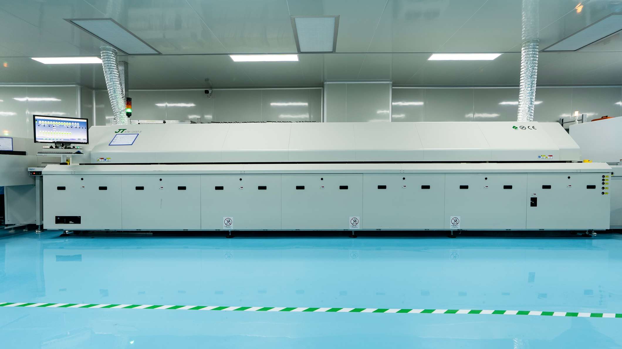
Reflow Ramp and Spatter
A ramp that is too fast boils the solvent in the paste before the flux has had time to act, and the escaping vapour carries metal with it. The spatter lands beside the joint and forms a ball.
The preheat section is where that is controlled. Our profile notes describe the measurement.
Moisture and Outgassing
Moisture in the laminate or in a component escapes during reflow and carries paste with it. A board that has absorbed moisture behaves differently from one that has just come out of dry storage.
Our bake schedule notes describe the handling that removes it.
Separating the Two Failure Modes
The useful distinction is whether the defect is attached. An attached bead is usually a mask or a pad geometry issue, and a detached ball is usually a paste handling issue. The inspection record should carry the distinction.
Where both appear together, the paste handling is the place to start. Our paste handling notes describe the routine.
Prevention
Prevention combines a stencil with an adequate area ratio, a cleaning interval matched to the print rate, a preheat that does not boil the paste and a controlled moisture state at the oven entrance.
Each of those is verifiable, which is what makes the defect controllable. Our squeegee notes describe the print parameters that go with them.
Verification
The verification is a count of balls and beads per board over a run, taken after each change, so that the effect of the change is visible in the data rather than in an impression.
Our acceptance criteria notes describe the limits that apply to the finished joint.
Process Control and Verification
On a design of this kind, solder bead is the item that decides how the rest of the board is arranged. The measurements that matter are the repeatable ones: conductor width and spacing, annular ring, finished hole size, plating thickness and surface finish are all verifiable on a coupon that travels with the panel. Running a first article through the same checks as the production panel confirms that the two agree, and that comparison is the cheapest form of process control available at prototype stage.
Keeping a sample from the panel turns a dispute into a measurement, because the same coupon can be re-examined by both parties without rebuilding the batch. Reviewing the design before the data is released is cheaper than correcting it after the panel is in the tank, because every step downstream inherits the decision made at the front end.
Documenting the assumption is part of the design work, and a short note on the drawing prevents a question that would otherwise arrive a day later and cost a day of schedule. The process window is set by the narrowest step in the flow, so an improvement anywhere else shows up as margin rather than as yield until that step is addressed.
A short note on the drawing about handling, storage or packaging is often worth more than an extra decimal place on a tolerance. Where a value sits close to a process limit, the drawing should say so, since the shop can then open the process window rather than working to a nominal figure that carries no tolerance.
A stack-up that is drawn rather than described removes most of the ambiguity from a quotation, and it lets the fabricator price the board against the dielectric and copper weights that will actually be used.
Process Control and Verification
On a design of this kind, solder bead is the item that decides how the rest of the board is arranged. The measurements that matter are the repeatable ones: conductor width and spacing, annular ring, finished hole size, plating thickness and surface finish are all verifiable on a coupon that travels with the panel. Running a first article through the same checks as the production panel confirms that the two agree, and that comparison is the cheapest form of process control available at prototype stage.
Keeping a sample from the panel turns a dispute into a measurement, because the same coupon can be re-examined by both parties without rebuilding the batch. Reviewing the design before the data is released is cheaper than correcting it after the panel is in the tank, because every step downstream inherits the decision made at the front end.
Documenting the assumption is part of the design work, and a short note on the drawing prevents a question that would otherwise arrive a day later and cost a day of schedule.
Process Control and Verification
On a design of this kind, solder bead is the item that decides how the rest of the board is arranged. The measurements that matter are the repeatable ones: conductor width and spacing, annular ring, finished hole size, plating thickness and surface finish are all verifiable on a coupon that travels with the panel. Running a first article through the same checks as the production panel confirms that the two agree, and that comparison is the cheapest form of process control available at prototype stage.
Keeping a sample from the panel turns a dispute into a measurement, because the same coupon can be re-examined by both parties without rebuilding the batch.
Process Control and Verification
On a design of this kind, solder bead is the item that decides how the rest of the board is arranged. The measurements that matter are the repeatable ones: conductor width and spacing, annular ring, finished hole size, plating thickness and surface finish are all verifiable on a coupon that travels with the panel. Running a first article through the same checks as the production panel confirms that the two agree, and that comparison is the cheapest form of process control available at prototype stage.
A first article check confirms that the process and the drawing agree on the points listed above, and that the coupon data supports the values used in the design.

Where a measurement falls outside the expected window, the sample is retained so that the cause can be established before the balance of the batch is released.
FAQ
Are small balls always a defect? Many standards accept a limited number of small balls where they are not between conductors and not in a critical area. The limit should be written down rather than assumed.
Does a nitrogen atmosphere help? It changes the surface tension and the oxidation, and it can reduce spatter, but it does not correct a stencil or a moisture problem.
What does gopcb provide against solder ball defects? We provide stencils specified by area ratio, a cleaning interval matched to the print rate, a verified preheat that does not boil the paste, a controlled moisture state before reflow, and a ball and bead count recorded per run so that any change shows up in the data.