
Solder Icicle Defects: 5 Causes in Wave Soldering
A solder icicle is a tapered spike of solder hanging from a joint after it has left the wave, and it forms when the alloy solidifies while it is still draining. The joint itself may be perfectly good. The spike is a projection that can break loose later, travel inside the product and create a short, which is why acceptance criteria treat it as a defect rather than a cosmetic issue.
Solder icicle defects are a wave soldering problem with a small number of physical causes. Solder drainage is driven by gravity and by the thermal energy still in the board. Anything that removes energy too early, or that leaves solder with nowhere to go, produces the same result: a joint that freezes mid-drain.
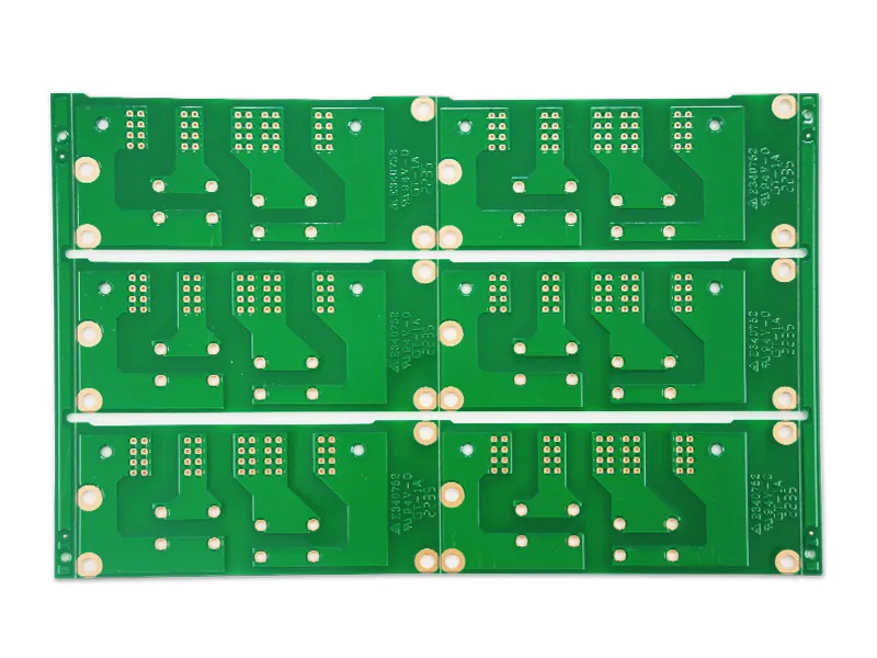
What a Solder Icicle Looks Like and Why It Matters
A true solder icicle is sharp, pointed and attached to the joint. It differs from a solder ball, which is spherical and usually not attached, and from a web or a bridge, which connects two conductors. The distinction matters because the causes and the fixes are different, and because a sharp projection is the version most likely to break free.
The risk is mechanical rather than electrical at the moment of manufacture. A spike that survives handling and assembly can be snapped by vibration, thermal cycling or a screwdriver during service, and the fragment becomes loose conductive debris inside a closed product. Workmanship standards such as the IPC requirements treat it accordingly.
Drainage: The Physics Behind the Defect
When the board leaves the wave, a fillet of molten solder is still attached to the joint, and solder drainage proceeds under gravity while the joint and the surrounding laminate give up their heat. If the alloy is still liquid when drainage finishes, the fillet becomes a normal joint. If it freezes first, the last part to leave remains as a spike.
So a solder icicle is the outcome of a race between solder drainage and freezing. Everything that speeds up drainage helps, and everything that cools the board or slows the flow hurts. That framing is useful because it explains why the same wave setting can produce icicles on a heavy board and clean joints on a thin one in the same panel.
Preheat Temperature and Flux Activation
Preheat temperature is the single most common cause. A board that reaches the wave too cool draws heat out of the solder as soon as it touches, so the fillet freezes early. A board that is too hot burns off the flux before it can reduce the oxide, and the resulting poor wetting leaves solder sitting on the surface where it can hang.
The top-side temperature at the wave should be measured, not inferred from the heater setting, and it should be recorded per product. Our notes on preheat and flux activation describe the measurement method and the windows that suit common flux types.
Conveyor Speed and Wave Contact
Conveyor speed sets the contact time between the joint and the wave, and contact time sets how much heat the joint takes on. Too fast, and the joint never reaches temperature; too slow, and the laminate absorbs heat it cannot shed, which can leave the board so hot that the solder stays fluid but the flux is gone.
Conveyor speed also controls the exit angle and the solder drainage window. A board that leaves the wave abruptly gives the solder less time to run off, and the spike that remains is thicker at the base. Raise or lower the conveyor speed in small steps and check both the fill and the drainage, because the two requirements pull in opposite directions.
Pallet and Board Design Effects
In wave soldering, pallets change the thermal map of the board and they can also trap solder. A pocket that fills with alloy during contact drains slowly and can leave material behind, and a pallet that masks a large area keeps heat away from the joints that need it. The direction of travel through the wave matters as well, because it decides which way a joint can drain.
At the design level, thermal relief on a ground plane and adequate spacing around a through-hole component help. Where the layout forces a heavy plane next to a small pad, the pad cools first and the solder on the heavy side keeps running, which produces the classic pallet and shadowing pattern of solder icicles next to clean joints.
Solder Pot Condition and Dross
Alloy contamination raises the liquidus and shortens the time available for drainage. Copper and other metals picked up from the boards accumulate until the pot is no longer within specification, so the same settings that worked last month produce spikes this month. This is one reason a solder icicle problem often appears as a slow drift rather than a sudden change.
Dross on the surface and around the nozzle has a similar effect, because it insulates the wave and reduces its heat. Pot analysis at a fixed interval, dross removal during production, and a record of what was added to the pot turn a vague complaint into a number you can act on. Our dross control notes cover the routine.
Nozzle, Wave Height and Flow
Wave height that is too low leaves the joints only partly immersed, which produces poor fill and a fillet that never merges with the wave. Wave height that is too high pushes alloy onto the board and creates turbulence, and turbulence is a source of both bridging and icicles because it leaves solder above the joint with no laminar path back into the wave.
In wave soldering the nozzle should be clean, correctly set for the board thickness and checked at the start of every shift. Height is normally maintained near half the board thickness above the surface, and the figure should be measured with the pump running under load rather than at idle. Details are in our wave height guide.
Fixing Icicles in the Right Order
Start with the profile: measure the top-side temperature and the contact time before touching any mechanical setting. Then verify the pot temperature and the alloy analysis, because contaminated alloy invalidates everything measured after it. Only then change conveyor speed, wave height and pallet design, and change one item at a time.
Where the wave soldering defect persists after those steps, look at flux type and application. A flux with the wrong activity for the alloy and the thermal load leaves oxide that the solder cannot wet, and no amount of profile tuning will fix an oxide problem. The full sequence for a wave soldering fault is set out in our process control notes.
Verification and Acceptance Limits
Verification should be visual, at magnification, on every board rather than on a sample, because a spike is easy to see once the inspector knows what a defect looks like. Boards should be checked after depaneling as well, since routing can create a projection of its own that is easily mistaken for an icicle.
Acceptance limits come from the workmanship standard and should be written into the drawing, with a note that loose solder debris is never acceptable. Where a projection is permitted in a coated area, the requirement should say so explicitly, and the reason should be recorded so the rule is not reversed by the next inspector.
FAQ
Can a solder icicle be removed and the board shipped? Only where the standard and the drawing allow rework, and only if the joint is re-profiled rather than cut. Cutting leaves a burr and a new stress point, and the cut material becomes loose debris, which is the very thing the defect was rejected for.
Why do solder icicles appear only on some boards in the same panel? Because the thermal load differs across the panel. A joint next to a large plane or a heavy component cools differently from one in open laminate, so the same preheat temperature and conveyor speed produce different drainage times in different locations.
Does a higher pot temperature solve the problem? Raising the temperature can help drainage, but it also increases oxidation and dross, and it can damage the laminate on long contact. Treat it as a small correction, not as the fix, and confirm the alloy is in specification before using temperature to compensate.