Solder Mask Dam And Sliver Defects
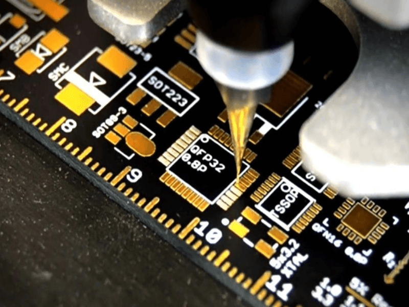
Solder mask is not a blanket that covers the whole board. It is a patterned layer that has to stop short of every pad that will be soldered, and the strip of mask left between two adjacent pads is called a dam. When that strip is narrow, or when the imaging process cannot resolve it cleanly, the feature either disappears or survives as a thin ribbon that is only loosely attached. Those two failures are the dam and sliver defects, and they are among the most common origins of a solder bridge in fine pitch assembly.
This article explains how dams and slivers are defined, how they arise from the imaging and development steps, what they do to a finished assembly, and which design and process rules hold them under control.
What A Dam And A Sliver Are
A dam is the solder mask strip that separates two solderable features. Its width is measured at the narrowest point, which is usually between the pads of a fine pitch component or between a pad and a via that sits close beside it. When the width falls below the resolution of the process, the strip is either not printed at all, leaving the two pads connected by exposed copper, or it is printed as a ribbon whose cross section is far smaller than the design intends.
A sliver is the extreme case of that second outcome. It is a narrow, elongated piece of cured mask that is attached to the board along one edge only, or that is held by a very small area at one end, and that lifts or breaks away during handling, during reflow, or during cleaning. Because a sliver is mechanically weak, it can survive fabrication and fail much later, which makes it a defect that inspection does not always catch at the source.
Registration And Resolution
Two different capabilities are involved, and they are often confused. Registration is how accurately the mask pattern is placed relative to the copper. Resolution is how small a feature the process can reproduce at all. A narrow dam can fail for either reason. If the artwork is correct but the mask is shifted, the dam loses width on one side. If the process cannot hold the dimension, the dam is thin even when it is perfectly placed.
Registration error accumulates from the artwork, the exposure, the copper etch, and the dimensional change of the laminate through lamination. On a board with a pad pitch of a third of a millimetre, a placement error of fifty micrometres is already a large fraction of the available dam, so the tolerance budget has to be built from the worst case combination rather than from the typical value that the process delivers on a good day.
How The Defects Form In Imaging
In a photoimageable process the mask is exposed through a film and the unexposed areas are washed away in development. A dam narrower than the resolution limit receives less exposure energy than a large area, because the light diffracts at the edge of the film feature, and the partially exposed material near that edge can be dissolved by the developer. The result is a dam that is thinner than designed at its base and that carries a rounded rather than a square profile.
Development is the second control point. Overdevelopment removes the partly cured material at the edges of small features and turns a marginal dam into a missing one, while underdevelopment leaves residue inside the pad openings. The development speed, the concentration, and the temperature all drift with production volume, and the drift is why a process that passes at the start of a run can fail at the end of the same run.

Why Slivers Matter In Assembly
A sliver that is still attached at fabrication can detach during assembly and land on a pad, where it acts as a spacer between the paste and the copper. The joint that forms is incomplete, and the defect shows up as an intermittent open or as a weak joint that passes electrical test and fails in the field. A sliver that stays in place is less dangerous, but it is a stress raiser and a place where the coating can lift during thermal cycling.
There is also an inspection cost. A sliver is a small feature that is difficult to classify, so it consumes inspection time and generates discussion about acceptance, and that discussion is harder to close when the fabrication drawing does not state a minimum dam width. Writing the number into the drawing is what turns a judgement call into a measurable criterion.
Design Rules That Prevent Them
The primary rule is a minimum dam width that the fabricator can hold reliably, typically around a hundred micrometres for a standard process and less for a fine line process. The designer sets the pad size and the pitch so that the remaining strip stays above that value, and checks the narrowest location on the board rather than the typical one. Defining the pads on a single grid keeps the dam uniform across the component, which matters because the narrowest dam on the panel sets the acceptance for the whole job.
The second rule is to avoid geometries that force a sliver. A mask strip that runs past the edge of a pad and ends in a point, or that fills an acute angle between two traces, is a sliver by construction. Rounding the end of the strip, widening it at the termination, and moving vias out of pad arrays remove most of the cases before they are drawn. The general geometry rules are collected under pad design standards and manufacturable design guidelines.
Process Controls And Inspection
On the process side the exposure energy and the development parameters are the levers, and both are best monitored with a test pattern that carries the same minimum feature as the product. A step wedge for exposure and a resolution target for development convert an invisible drift into a number that can be trended before product is lost. The ink itself also matters, because its rheology sets how sharply the printed edge forms, as described under solder mask ink thixotropy.
The standard approach to acceptance is a visual inspection under magnification against a written criterion. A dam that is below the minimum width but continuous, and that is firmly attached along its full length, is usually accepted. A dam that is broken, or a sliver that is loose or partially lifted, is rejected. Applying that rule consistently is only possible when the drawing states the minimum width, the inspection magnification, and the lighting condition, so the fabricator and the customer are looking at the same thing.
FAQ
Is a narrow dam always a defect? No. A dam below the nominal minimum but continuous, firmly bonded, and free of pinholes is normally accepted, because it still separates the pads and does not lift during assembly.
Can a sliver be repaired? A loose sliver cannot be reattached reliably, because cured mask will not bond to the surface again. The practical remedy is to remove it and to correct the artwork or the process so the feature is not produced.
Does a finer mask process solve the problem? It raises the resolution and lowers the achievable dam width, but it does not change the registration budget. Both capabilities have to hold before a fine pitch dam becomes manufacturable.